A MOS 6502 CPU rebuilt from 4,051 individual transistors. No chips and no FPGA.
The board reproduces the original silicon die, transistor for transistor.
The MOS 6502 powered the Apple II, the Commodore 64, the NES and the BBC Micro.
Roughly 3,500 transistors sit inside its package, on a fingernail of silicon.
This project takes that exact circuit and rebuilds it from parts you can see.
Every transistor becomes a separate SOT-323 package. The board is the size of a
sheet of A4 paper.
It is not a simulation and not an emulation. The logic is the real thing.
It is the same dynamic NMOS circuit that the original used, and it runs the same
instructions. It is a few thousand times larger and a few hundred times slower.
the boardthe die← move across →
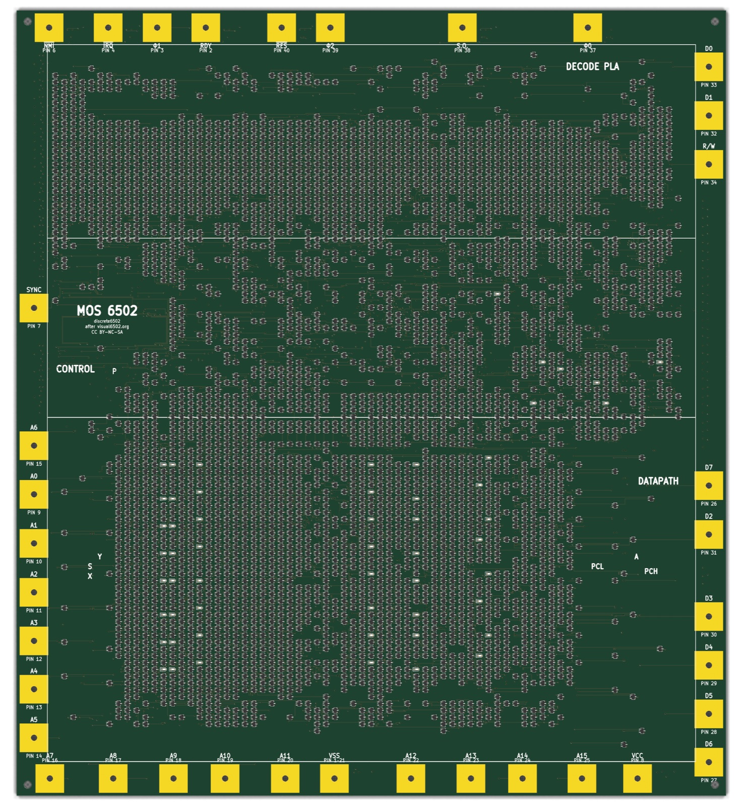
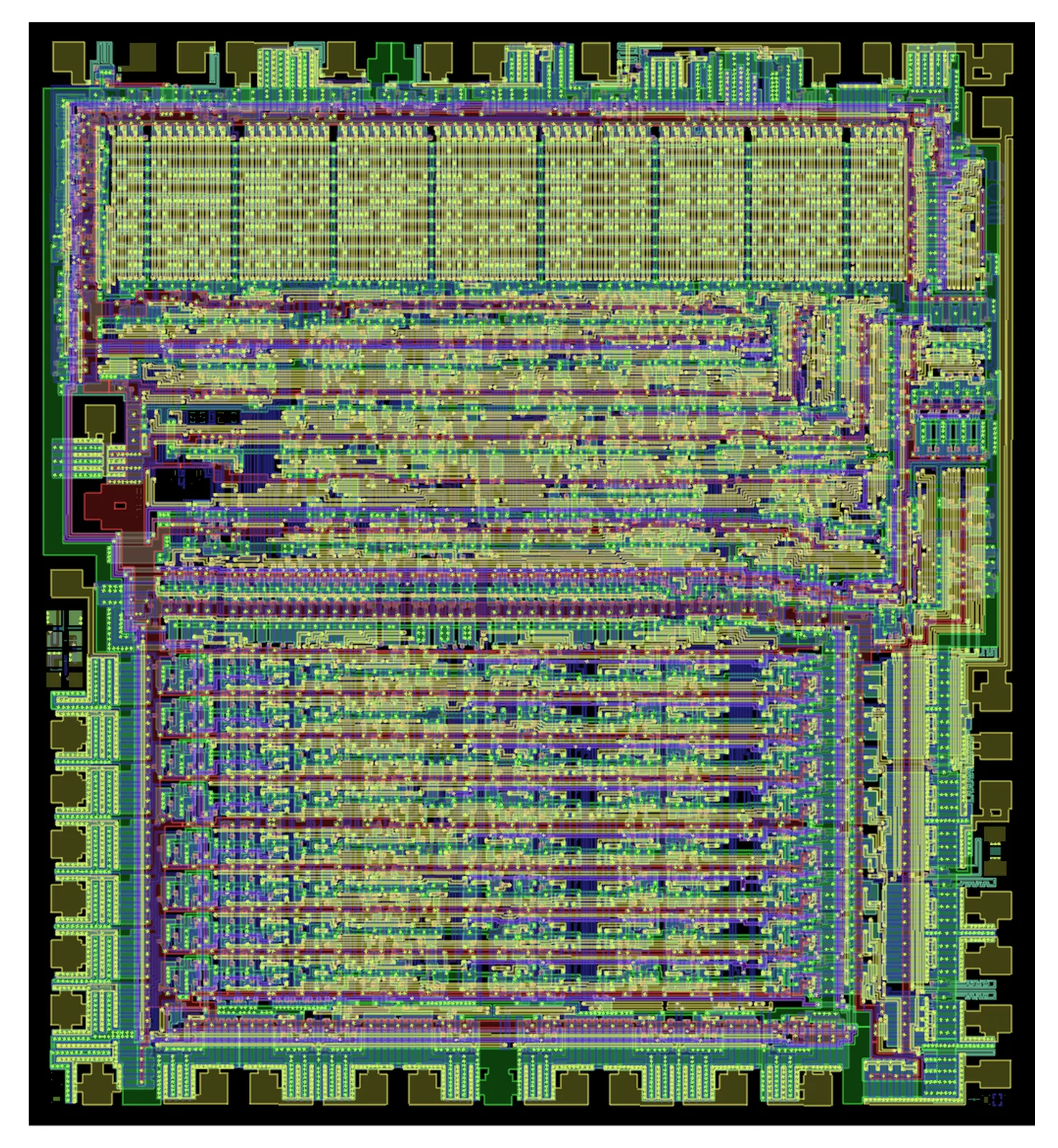
The same object twice: this board on the left, and the traced silicon of a real 6502
on the right. The die render uses the board's own die-coordinate transform. The blocks
line up because the parts sit where the silicon put them.
The die layers come from visual6502,
photographed from a MOS 6502 revision D in 2009. The project data is CC BY-NC-SA.
The layout
The board is the die
Each part sits at the coordinates of the transistor it replaces, scaled up from
photographs of a real decapped 6502. Nothing about the arrangement is decorative.
The stripes, the clusters and the empty channels are the floorplan of the chip itself.
They appear because the parts go where the silicon put them.
The front face carries only transistors and LEDs, so the texture reads cleanly.
Every resistor and capacitor lives on the back.
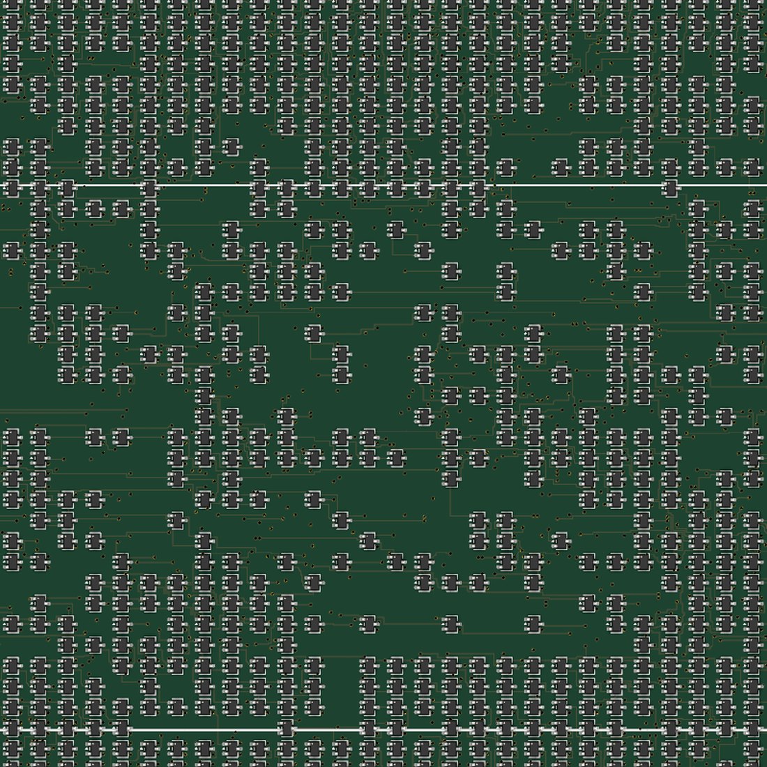
Detail: individual SOT-323 packages. The density variation belongs to the die, not to a designer.
Decode PLA
The instruction decoder. It is the dense, regular stripes across the top third.
Each input line drives up to 71 separate transistor gates.
Datapath
Registers and the ALU, in the ordered columns along the bottom. Bit lanes run
horizontally, exactly as they do on silicon.
Bond pads
36 gold pads sit at the real bond-pad positions of the die. Each one is 11.6 mm
square and drilled for a crocodile clip. The silkscreen labels them with the classic
DIP-40 pin names.
55 LEDs
One LED per register bit: A, X, Y, the stack pointer, both halves of the program
counter, and 7 status flags. The LEDs show the CPU state while it runs.
How it works
Faithful, not modernized
The easy version of this project converts the 6502 to modern static logic and calls it
done. This one does not. It keeps the original dynamic NMOS design. In that design
a wire stores data as charge on its own capacitance. The clock must refresh that charge
before it leaks away.
Pull-ups, not depletion loads
The depletion-mode load transistors of the original have no discrete equivalent.
1,023 resistors of 10 kΩ take their place. They were long assumed to consume nearly all the power — wrongly: they draw 1.3 W of the board's ~10 W, and eight other transistors burn most of the rest. See the status note below.
Pass gates, doubled
778 of the transistors pass signals in both directions. A 3-terminal part cannot
do this. Each one becomes a back-to-back pair, so 1,556 transistors do the work of
778.
The bootstrap trick
A pass gate should lose a threshold voltage. It does not. The clock edge couples
through the gate and pushes the stored '1' above the supply rail. SPICE
confirms this with the manufacturer's own model.
Honest about speed
Roughly 10 kHz to 20 kHz, against 1 MHz for the real chip. One 10 kΩ resistor
needs microseconds to drive 71 gates. Slow is the point. You can watch it think.
The clock is bounded at both ends. A dynamic node stores a bit as charge, so the
clock must refresh that charge before it leaks away. That sets a floor as well as a
ceiling. The weakest node on the board holds 32 pF against twelve leaking transistors.
If each transistor leaks the typical 1 nA, the floor sits near 380 Hz, far below the
ceiling. At the worst leakage the datasheet permits, 500 nA, the floor would rise to
187 kHz and cross the ceiling. No clock speed would work at all. Simulation cannot
resolve currents that small, so this had to be measured — and on 2026-08-23 it was:
1.9–2.3 nA per transistor, from filming two accumulator LEDs fade at 120 frames a
second on nets that have no connection to either supply rail, so leaking is the only thing
that can turn them off. The floor is 456–871 Hz against a 20 kHz ceiling — a usable
window of 23 to 44 times, with about 45 °C of temperature headroom. The
firmware can also measure it the deliberate way. It stops the clock, restarts
it, and finds the point where the CPU forgets itself.
Method
Nothing was drawn by hand
At 5,421 components and 8,421 connections, hand-drawing a schematic is not slow.
It is impossible. Every stage is
a script. One command
per stage regenerates the whole board from the source data.
Start from the real chip. The visual6502 project photographed and traced an
actual 6502 die into a transistor-level netlist. That is the ground truth. It is not a
datasheet and not a reimplementation.
Transform it. Merge redundant parallel transistors, expand bidirectional
pass gates into pairs, turn pull-up markers into resistors, add LED taps and
protection.
Place by die coordinate. Each part goes where its transistor sits on the
silicon. A part moves only as far as a collision requires, a median of 1.5 mm.
Route it. Off-the-shelf autorouters failed. One managed 700 of 8,500
connections in ten hours. A purpose-built negotiated-congestion router finished all
8,421 across four routing layers.
Prove it. Five independent checks run from logic down to copper, before
anyone orders a board.
Verification
Five gates, all green
You cannot debug a board this size by probing it afterwards. Every check therefore
runs before fabrication, and again on every change.
Check
Result
Switch-level simulation against the original netlist
identical traces
Board matches the generated netlist
0 errors
Independent copper connectivity trace
0 broken nets
Manufacturer design-rule check
0 electrical violations
Netlist rebuilt from the copper, then simulated
0 opens, 0 shorts, runs correctly
The last gate runs backwards. Every other check reads the design forwards.
Each one trusts the record that the CAD tool keeps of what connects to what. This gate
throws that record away. It reads the finished board as raw copper: pads, tracks, vias
and the power planes. It finds which pieces of metal touch, and it rebuilds the circuit
from that alone. The rebuilt circuit then executes 6502 instructions. visual6502 did the
same thing to real silicon. To prove that the gate can fail, we cut one track. The gate
reported exactly one broken net, by name.
The equivalence test runs real code. One program uses the stack, subroutine
calls, arithmetic and branches. It runs on the original visual6502 netlist and on this
transformed one. Every signal must match on every cycle. If it does not match, the
change fails.
And here is what all five of them miss. Every check above asks whether the right
things are connected. None of them asks whether they are the right strength.
A simulator that decides a wire is low whenever anything pulls it low will happily approve a
circuit where the thing pulling down is no stronger than the thing pulling up — the
wire never actually gets there. That is not a hypothetical: it is exactly the flaw described
in the status section below, sitting in this design through five green gates. Verification
tells you what it was built to ask, and its silence is not agreement.
Bring-up
It brings its own computer
A CPU alone does nothing. It needs a clock and memory. Both live on the back of the
board, as an unpopulated footprint for a Raspberry Pi Pico 2 W. The footprint wires to
the data bus, 14 address lines, reset, read/write and SYNC.
Solder a Pico on and flash the firmware. The Pico then becomes the clock master and a
memory emulator. It serves every instruction fetch, captures every write, and traces the
bus cycle by cycle. You need no other equipment. Board #1 has had one since
2026-08-25, and it is what the CPU is running from in the clip below.
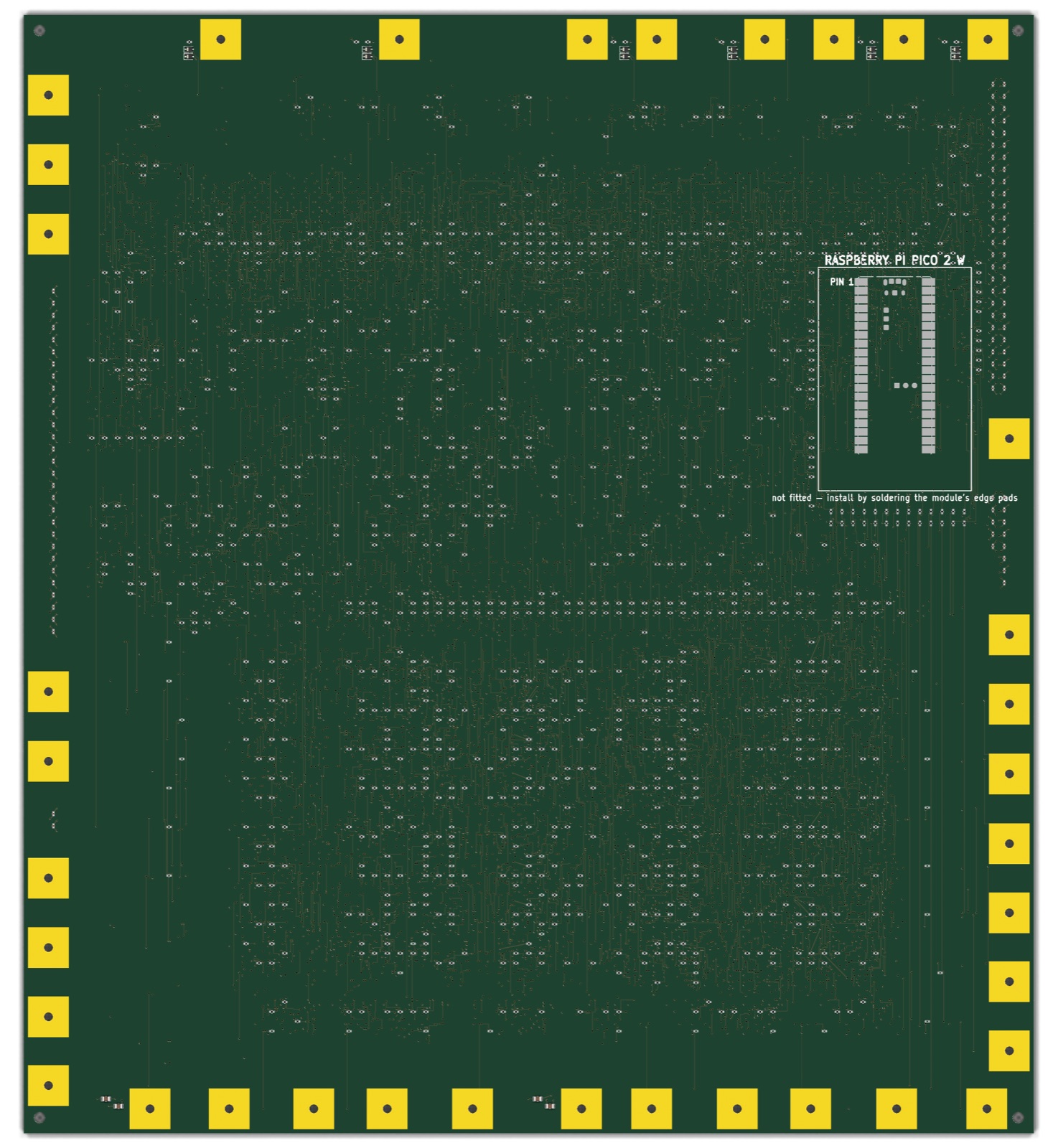
The back: 1,023 pull-up resistors, 96 decoupling capacitors, and the Pico site in the natural gap of the die
Specification
By the numbers
Item
Value
Transistors
4,051 (3,996 logic + 55 LED drivers)
Transistor type
BSS138W, SOT-323
Pull-up resistors
1,023 × 10 kΩ
Register LEDs
55
Total components
5,421 across 2,624 nets
Board
290.7 × 322.0 mm, 6 layers, ENIG
Routing
8,421 connections · 103 m of copper · 14,454 vias
Supply
5 V (3.3 V also validated)
Power
1.70 A running, 0.30 A stopped (measured) · the difference is contention, rework pending
Clock ceiling
≈ 20 kHz at 5 V, ≈ 10 kHz at 3.3 V
Clock floor
456–871 Hz measured on board #1 (leakage 1.9–2.3 nA/FET)
Status
It works, and it is not finished
The boards arrived on 2026-08-12. On 2026-08-25 one of them executed a program from its own
Pico — 4,051 discrete transistors fetching, decoding and running instructions, with
the accumulator counting in LEDs. What is left is the part that decides whether it is a 6502
or merely something that looks like one: does it execute every instruction correctly?
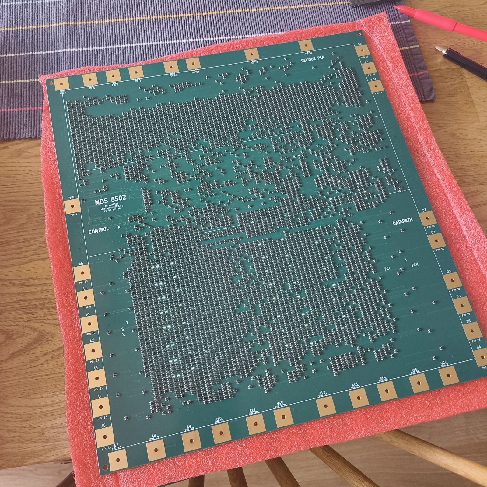
As delivered, 2026-08-12. Every dark speck is one of 4,051 transistors, placed
where its counterpart sits on the real die. The pen gives the scale: the board is
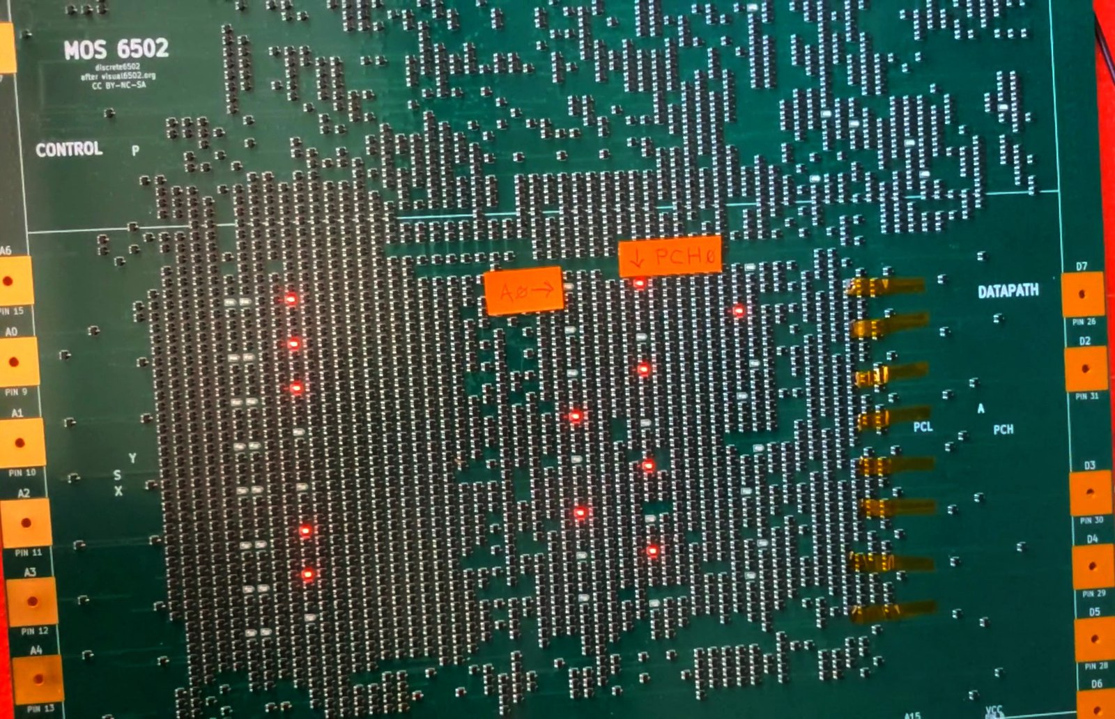
29 cm across.Running. The lit LEDs are register bits — the orange labels mark
A0 and PCH0, written on by hand so the program counter could be identified
by name in video rather than inferred from a spectrum. The amber patches down the
right of the array are Kapton tape over the eight hand-reworked data-bus drivers, insulating
each added resistor from the transistor leg lifted to make room for it.
Two worries carried all the way from design are now settled on hardware. The dynamic
logic holds its charge on long board traces instead of microscopic silicon nodes —
leakage measured 1.9–2.3 nA per transistor against a 53 nA budget, so the clock
window is real, and wider than the simulation could prove. And the bootstrap effect that the
whole pass-gate scheme depends on had been simulated but never soldered; the
program counter was found counting, four LEDs identified by name blinking at exactly
the frequencies arithmetic demands, each at half the rate of the one above it. Neither was
provable before the boards existed.
Rev A has a real flaw, and the board is running in spite of it. The transform that
turned the die's netlist into a board preserved every connection faithfully, but not
every device ratio. This style of logic needs a deliberately weak pull-up fighting a
strong pull-down; the 1,018 obvious cases became 10 kΩ resistors, but 164 transistors kept
the same part as the transistors pulling against them — a fair fight where the design
needs a rigged one. A contended pair burns about 0.9 W in a package rated for 0.3 W, and
leaves a logic “low” sitting at 1–1.9 V when the receiving gate switches at
1.1–1.5 V. Measured on board #1: 1.70 A executing against 0.30 A with the clock stopped. The stopped figure is the passive network behaving exactly as designed (0.35 A predicted); the 1.40 A difference is contention, about 180 mA in each of the handful of nets contending at any moment.
It was found by asking a question with no obvious connection to it: does the MOnSter 6502
have a minimum clock speed? Its designer's answer described a failure we had not
considered, which prompted re-deriving our own numbers rather than assuming the two designs
behaved alike. The confirmation is almost embarrassing in hindsight — the MOnSter 6502
has always published about 2 A and 10 W for the same style of logic, and the measured figure
here landed within 15% of it. Our own estimate had said 1.6 W, six times lower, and nobody had
asked why the same circuit should be six times cheaper.
The repair works, and that is now measured rather than argued. Eight transistors driving
the data bus were reworked by hand — one resistor each, all on the front face in a single
column,
here is exactly how, site by site. A thermal camera then
confirmed it in a way nobody had planned: under the workload where those eight contend
91.8% of the time, they run cold. Unreworked, that would have been 7 W in eight
SOT-323 packages and impossible to miss.
The same camera then found sixteen more. The address-path drivers carry the identical
defect and were never reworked; nine of them measure about 80 °C while the board
executes real code. All sixteen contend in normal use: adhis the high byte of
the address during a fetch, so each bit is pulled low about half the time as the address
sweeps. Confirmed on 2026-08-26, when a free-run of NOPs ran every one of them hot and the two
slowest bits were seen cycling hot and cold at exactly the rate the program counter
dictates.
All sixteen are mapped, with the duty cycle measured for each and the same site-by-site procedure. The generator can also emit the fix at all 142 vulnerable sites for a future revision.
The flaw is recorded rather than quietly patched, because the interesting part is not
the bug. It is that five green verification gates could not see it. They all check
topology. None of them checks strength — the switch-level model
resolves any contention as a clean low, because it assumes the pull-down wins. A camera
pointed at the real board has now corrected that model twice, once by finding heat the
simulation said was absent, and once by finding heat at transistors the analysis had excluded
from the search altogether.
What remains. A free-run never touches the ALU, the registers, the stack, the flags,
addressing modes or branches. The acceptance gate is
Klaus Dormann's 6502 functional test suite — about three hours at this clock,
already built and passing in an emulator against the same mirrored 16 KB memory the hardware
presents, so if the board fails it, the board is what failed. It waits on the address-path
rework.
Every measurement, in the order it was taken, with the reasoning that resolved each surprise
— a reading that looked like a short and turned out to be 1,899 body diodes; a
retraction that was itself retracted —
bring-up as it actually happened. The procedure it was
supposed to follow is here, step by step.
 the board
the die
← move across →
the board
the die
← move across →