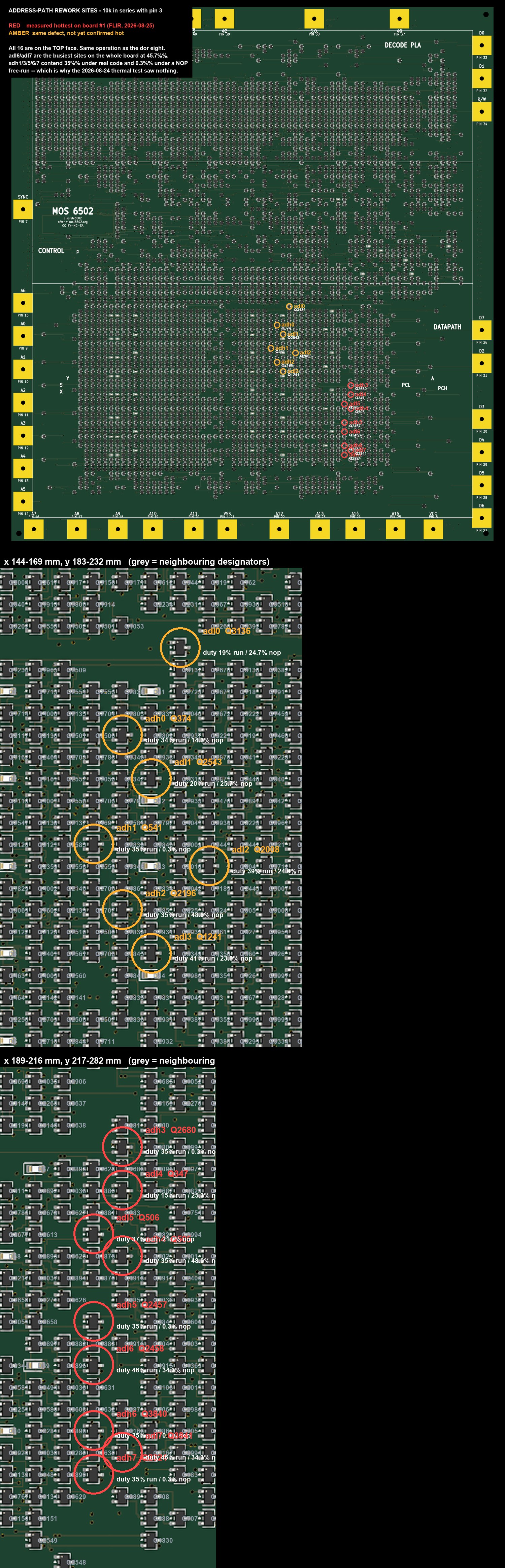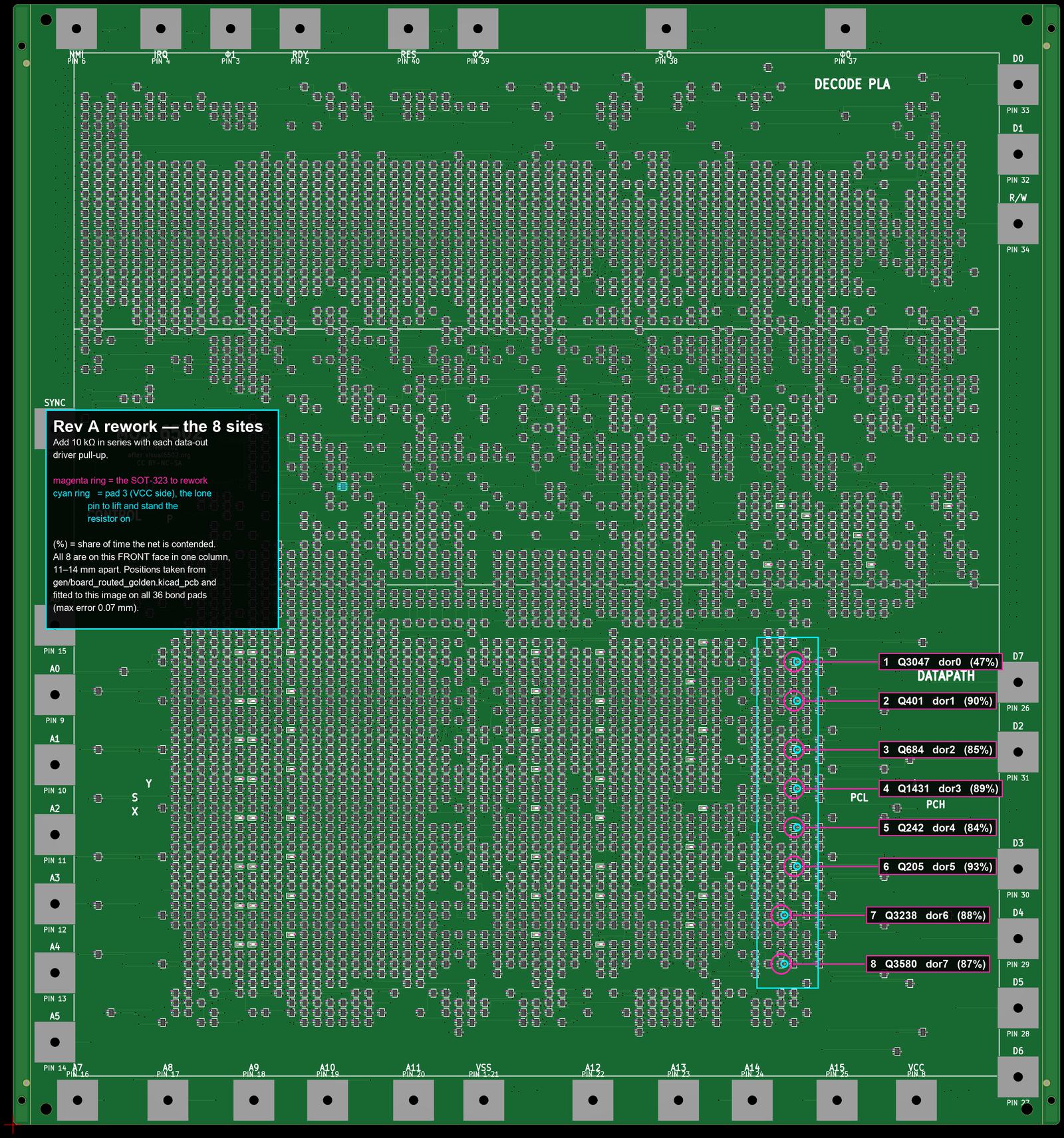
gen/board_routed_golden.kicad_pcb; the mm-to-pixel mapping was fitted on
all 36 bond pads, worst error 0.07 mm against a 0.65 mm pad pitch. Click to enlarge.discrete6502 — generated from gen/board_routed_golden.kicad_pcb.
Background and measurements: “Driver contention” in project-plan.md,
sim/driver_contention.sp (the defect) and sim/revb_driver.sp
(the fix, simulated).
Ratioed NMOS needs the pull-down several times stronger than its load. The transform turned the 1,018 depletion loads into 10 kΩ resistors — correct — but left the eight data-bus output drivers with a BSS138W as the load against a BSS138W as the pull-down: a 1:1 ratio where the die had a deliberately weak load. Measured consequences at 5 V:
RnWstretched holds the pull-down
on through every read while the stale dor bit holds the pull-up on.Adding 10 kΩ in series with each pull-up restores exactly the ratio the other 1,018 nodes already have: 0.5 mA instead of 262 mA, and a low of ~3 mV. There is no speed cost — each of these nets drives exactly one gate (27 pF), so 10 kΩ gives a 0.6 µs rise against a 25 µs half-cycle.
sim/revb_driver.sp measures this exact modification on a driver taken out of
gen/netlist.json rather than an invented one — dor1 → Q401 →
n798 → Q192 → db1, the worst of the eight (90% duty), carried
two stages deep to the actual data-bus output pad, so the fix is judged by what leaves the
CPU rather than by the node the resistor sits on. Before and after, same devices, same models:
| At 5 V | As built | With the 10 kΩ |
|---|---|---|
| Contention current | 262 mA | 0.499 mA — 525× less |
| The contended “low” | 1.86 V — invalid | 2.9 mV — valid |
| db1 rise to 1.5 V | 18 ns | 271 ns — 90× inside a 25 µs half-cycle |
| db1 fall | 2.8 ns | 2.7 ns — unchanged |
| db1 high level | 3.81 V | 4.38 V |
| Peak supply current, one cycle | 346 mA | 0.92 mA |
The same run also settled a question about the fallback option below. At 3.3 V with worst-case Vth (1.5 V, the datasheet maximum), the un-reworked board’s db1 stops at 1.306 V and never reaches the 1.5 V threshold of the gate it has to drive; reworked, it reaches 1.579 V. Two source followers in series subtract Vth twice. So running at 3.3 V is not a way to avoid the rework — the rework is what makes 3.3 V viable.
gen/board_routed_golden.kicad_pcb; the mm-to-pixel mapping was fitted on
all 36 bond pads, worst error 0.07 mm against a 0.65 mm pad pitch. Click to enlarge.All eight are the same part (BSS138W, SOT-323) in the same orientation (0°), with identical copper around them. Board origin is top-left; x increases right, y increases down, matching KiCad.
| Signal | FET | Pad 3 (VCC) centre | Its VCC via | Node |
|---|---|---|---|---|
| dor0 | Q3047 | 220.24, 189.00 | 220.40, 189.75 | n1325 |
| dor1 | Q401 | 220.24, 200.20 | 220.40, 200.95 | n798 |
| dor2 | Q684 | 220.24, 214.20 | 220.40, 214.95 | n520 |
| dor3 | Q1431 | 220.24, 225.40 | 220.40, 226.15 | n42 |
| dor4 | Q242 | 220.24, 236.60 | 220.40, 237.35 | n1076 |
| dor5 | Q205 | 220.24, 247.80 | 220.40, 248.55 | n373 |
| dor6 | Q3238 | 216.54, 261.80 | 216.70, 262.55 | n7 |
| dor7 | Q3580 | 216.54, 275.80 | 216.70, 276.55 | n298 |
Note dor6 and dor7 sit 3.70 mm to the left of the other six. Nearest neighbouring component at every site is 1.94 mm away, so there is working room.
dor n), pad 2 the source feeding the node, pad 3 the drain that reaches
VCC through the short track and the via below it. Pad 3 sits 1.78 mm from the other two, alone on
its side of the package — which is what makes lifting it low-risk. In the AFTER panel the leg
is off its pad, so the track to the via is dead copper (dark), and the 10 kΩ stands on pad 3
with the lifted leg soldered to its top.
These are renders generated from gen/board_routed_golden.kicad_pcb,
not photographs — no board exists yet. Every pad, track and via below is real board geometry, drawn
at true scale, front face, 8 × 8 mm around each target. Use them to identify the right part among
its identical neighbours before you touch anything.
Gold = copper pads and vias · brighter gold = the target FET's own pads, numbered · yellow tracks = VCC · blue = VSS · red circle = the pull-up FET · red bar = the 0.75 mm pad-3 track to its VCC via · green labels = neighbouring parts · scale bar = 1 mm.
Parts: eight 10 kΩ resistors. 0402 is what the board uses (LCSC C25744) but 0603 is easier to handle and there is room — nearest neighbour is 1.94 mm away. Tools: fine-tip iron or hot air, fine tweezers, flux, magnification, a multimeter.
W in the tester, or the wifi panel's find the boundary) should be measured on
the board in its final electrical state. Two reasons. First, the stall test is safer after
the fix: freezing the clock is exactly the condition that parks a pull-up and a pull-down
on together, and on these eight nets the fix drops that from 262 mA to 0.5 mA. Second,
a number taken before the fix would not be the number you carry forward — eight
drivers dissipating ~0.8 W each warm the board, and leakage roughly doubles every 10 °C,
so a pre-rework floor would read pessimistically and for a reason that no longer applies. If you do
measure both, keep both: a floor that moves after the rework is telling you the eight sites were
heating their neighbours, which is worth knowing. Either way the safety rules in
pico-controller/README.md still apply — current-limited supply, 3.3 V first,
sub-millisecond stalls ramped up.
tools/contention_duty.py,
which makes the exact figure soft though not the direction), so
unreworked they would burn ~7 W between them and be the hottest thing on the board by far. On
board #1 they are cold in exactly that condition. If any of the eight shows up warm
under NOPs, that site did not take — and the Kapton in step 5 exists to stop precisely that.DISCRETE6502_REV_B=1 python3 tools/gen_netlist.py emits
the series resistor at 142 sites — every VCC-side FET that has a pull-down to
fight — sized per net from its own gate load, because a blanket 10 kΩ on the heavy clock
nets would give a 286 µs rise and destroy the clock. Simulated too: the clock net keeps
its level to within 2 mV and rises 25× inside a half-cycle. One caveat if it is ever
fabricated — the two 100 Ω sites (cclk, cp1) dissipate
200 mW while contended in an 0402 rated 0.0625 W, so use 0805 there. That is a
respin, not a patch.