discrete6502 — the measurement log for the real boards. This page records
what was measured and what it meant. The procedure — what to do, in what order, and why —
lives in bringing the board to life. Where the two disagree, this page
is the record of events and that page is the instruction; both get corrected.
Why this page exists. The very first measurement of the project disagreed with its
own written gate, and the disagreement was the procedure's fault, not the board's. That is worth
capturing while it is fresh: a number that looks alarming, the reasoning that resolved it, and the
correction it forced upstream. Everything here is dated and attributed to a specific board.
Progress
Step
Date
Board
Result
0 — Receiving inspection
2026-08-12
all
PASS
1 — VCC↔VSS resistance, unpowered
2026-08-12
#1 (all four, forward)
PASS
2 — 5 V, unclocked, no Pico
2026-08-23
#1
PASS — but 1.4 A, 4× budget
2b — Charge retention (by video)
2026-08-23
#1
PASS — 1.9–2.3 nA/FET
3 — External clock, watch the LEDs
2026-08-24
#1
PASS — clock regenerates on-board
3b — Thermal map (FLIR One)
2026-08-24
#1
no hot spots — model corrected
3c — Does it compute? (PC ripple)
2026-08-25
#1
PASS — the CPU executes
4 — Eight-site 10 kΩ rework
2026-08-23
#1
done (out of order)
5 — Solder the Pico
2026-08-25
#1
PASS
6 — First clocked run off the Pico
2026-08-25
#1
PASS — A counts; 2.3 A, contention found
6b — NOP-workload thermal test
2026-08-26
#1
prediction failed, mechanism survived
6c — Supply current, stopped vs executing
2026-08-26
#1
0.30 A / 1.70 A
7 — Clock window
—
—
not yet run
8 — Functional test
—
—
not yet run
PassStep 0 — Receiving inspection, 2026-08-12
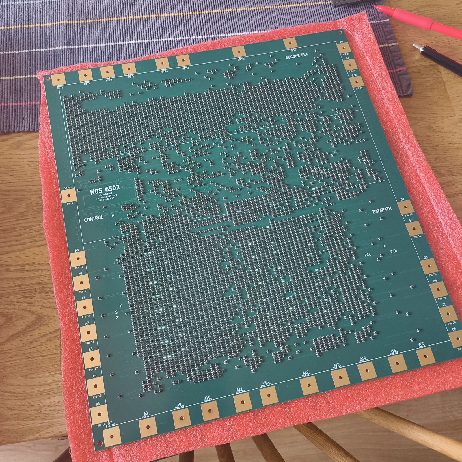
Boards arrived: 4 assembled, 1 bare, as ordered. Depaneled by JLC, so the 5 mm process rails
are already gone. Visual condition good on all four.
Top face. The die floorplan reproduces itself out of component
placement alone — decode PLA across the top, control in the middle band, datapath below. The
empty space is deliberate: refusing to pack the transistors is what keeps the texture readable
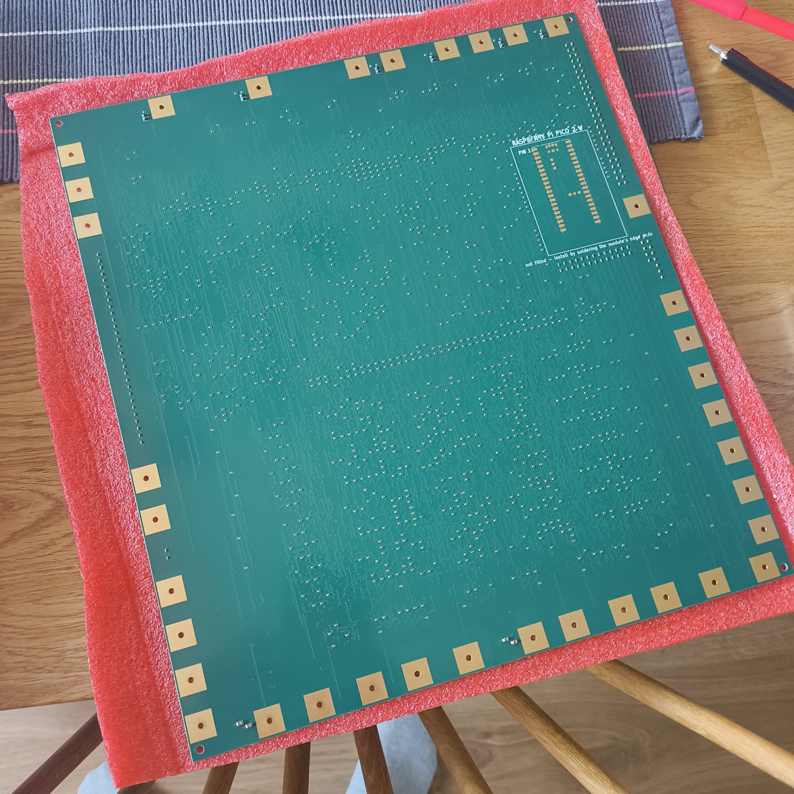
and, incidentally, what keeps the board locally sparse enough to assemble easily.Underside. The Pico 2 W site is silkscreened but unpopulated, as
designed. The back also carries every passive on the board — roughly a thousand 0402 resistors —
but at this scale a 0402 is a few pixels and indistinguishable from a via. That is why Step 1
matters more than this photograph.
What the close-up inspection actually confirms, beyond “it looks nice”:
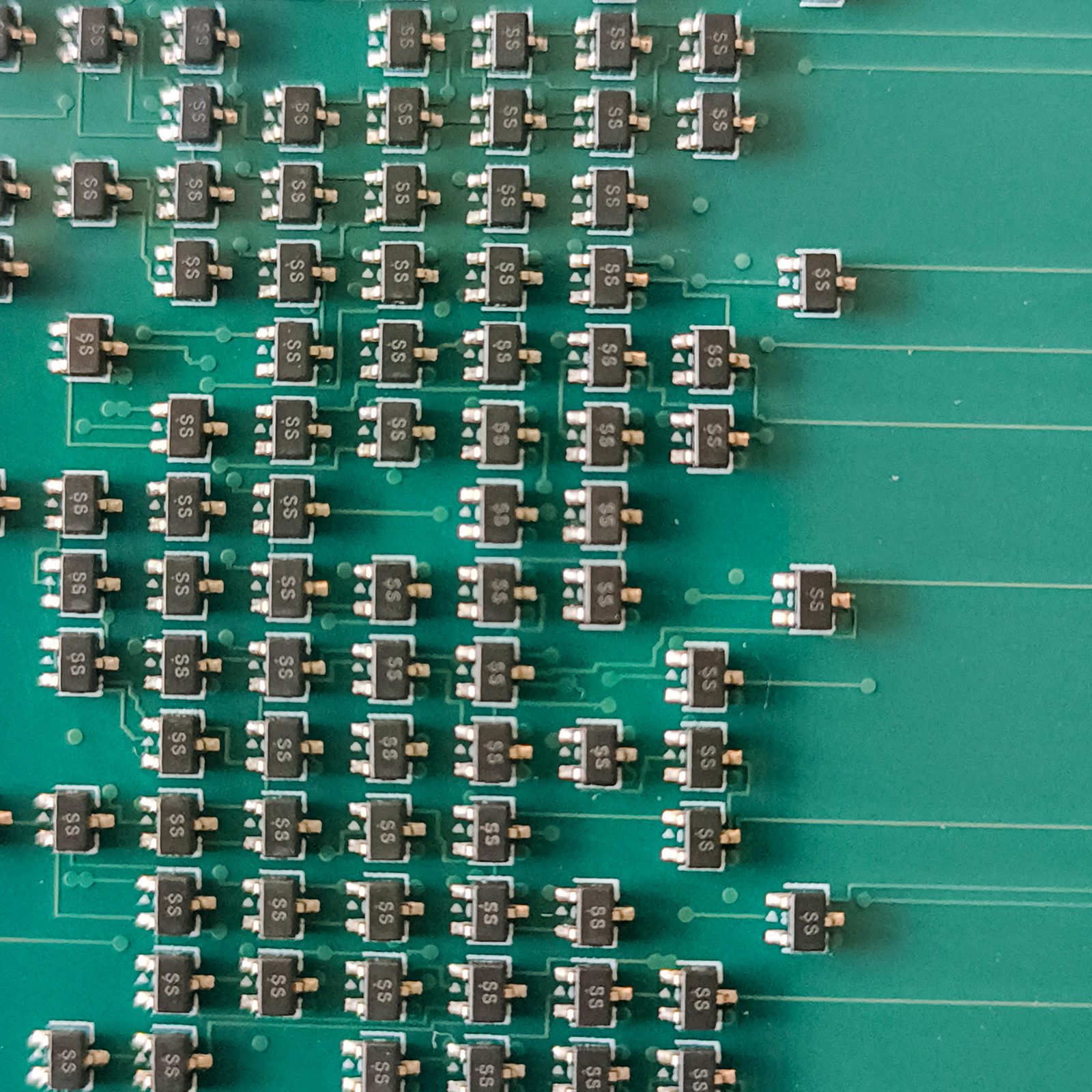
FET orientation is uniform across the array. Every SOT-323 sits the same
way round, pin-1 marker against the silk triangle, matching the all-0° rotation recorded in
“Placement verified from JLC's DFM” in project-plan.md. That check was made on
a DFM render before production; this is the same check on delivered hardware, and it closes
the risk that would have taken out all four boards at once.
One marking code throughout. Every transistor carries the same top mark, so
the array came off one reel — consistent with a single line item and against the
wrong-reel-on-one-feeder failure.
Fillets are formed and consistent at the magnification available, with no
visible bridging between the 0.65 mm SOT-323 pins and no tombstoning in view. This is a
sample of a few dozen parts out of 5,328, so it is encouraging rather than conclusive; the
defects the yield estimate predicts are singles, and singles are not found by eye.
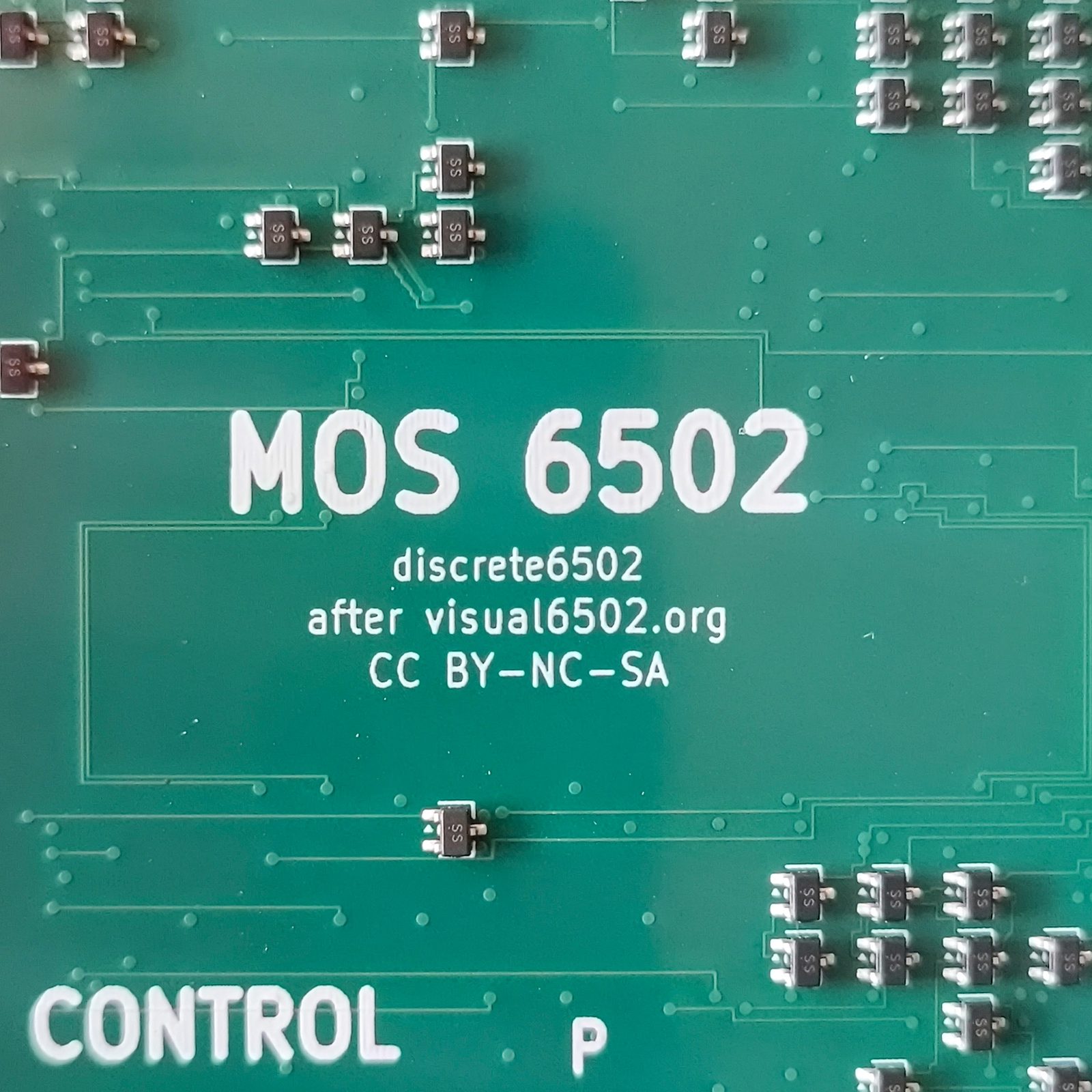
Silkscreen is legible and correctly placed — the die-block labels, the
bond-pad names, and the MOS 6502 / discrete6502 / after visual6502.org / CC BY-NC-SA
block all print cleanly, which retires the concern behind the rev A silk re-placement (text
crossing pad copper was being printed half-eaten).
The evidence, close up. Every package is oriented identically and
every one carries the same top mark. The silk triangle beside each part marks pin 1; the
package's own pin-1 corner lines up with it throughout. This is the rotation check from JLC's
DFM render, repeated on delivered hardware.Silkscreen quality. Crisp edges, no fill-in, nothing eaten by a
pad opening — which is what the rev A silk re-placement was for. Attribution to visual6502.org
and the CC BY-NC-SA notice are on the board itself, where they belong.
Not verified visually: the underside passives. At photographic scale a 0402
resistor on a green board is a few pixels and is easy to mistake for a via — compare the underside
photo above. This did not need resolving by eye, because Step 1 settles it electrically: see
“Step 1 is a positive test” below.
The empty pads on the back are meant to be empty
Besides the Pico site there are 56 unpopulated 0402 capacitor footprints,
C101–C156, and they are correct. They are the DNP ballast capacitors added
as layout insurance in M4 (2026-07-18), one per bit on each of the six buses:
Bus
Bits
What it is
sb0–7
8
special bus — internal
idb0–7
8
internal data bus
adl0–7
8
address low
adh0–7
8
address high
db0–7
8
data bus
ab0–15
16
address bus
They were never in the BOM or the CPL, so the assembler was never asked to place them. The
census reconciles exactly, which is the real answer to “did they miss something?”:
The CPL splits 4,106 top / 1,222 bottom, and the 100 capacitors it does place on the bottom are
the 96 decouplers plus 4 bulk — so every part that was supposed to be fitted, was.
Keep these pads in mind at Step 7. They are not decoration: sb0–7 are
the worst dynamic nodes on the board — no pull-up at all, 13 FET pins hanging off each, and
the 32 pF that sets the retention floor (see tools/dynamic_nodes.py and the clock-floor
entry in project-plan.md). If the measured retention floor comes out too close to the
clock ceiling, these footprints are the built-in remedy — hand-fitting 100 pF on the
sb bits multiplies that node's stored charge several-fold. It is a trade, not a free
win: more capacitance buys retention at the cost of slewing the node more slowly, so it lowers the
ceiling while lowering the floor. Decide it with the Step 7 numbers in hand, not before.
Instrument: Biltema 2000018521 handheld DMM, manual range. Probes on a VCC bond pad and a VSS
bond pad. “Forward” below means red probe on VSS — the direction the FET body
diodes conduct. “Reverse” means red on VCC, which is also the board's normal operating polarity.
What was read
Range
Forward (red on VSS)
Reverse (red on VCC)
200 Ω
195 Ω
OL (over range)
2000 Ω
314 Ω
595 Ω
20 kΩ
3.77 kΩ
8.21 kΩ
All four boards read ≈195 Ω forward on the 200 Ω range. The reverse reading was held for ~20 s
and drifted slowly down, 8.21 → 8.18 kΩ.
Verdict: PASS. This is a healthy board, and the guide's gate was wrong.
Why 195 Ω is not a solder bridge
Four independent arguments, in increasing order of how much they depend on modelling:
A rail bridge cannot read 195 Ω. VCC and VSS are solid inner-layer planes
joined by thousands of stitching vias. Solder shorting them reads a fraction of an ohm.
195 Ω is three orders of magnitude too high.
All four boards agree. A solder bridge is a random defect. Four boards
landing on the same number is a property of the design, not of the assembly.
The reading changes with range. The same two points read 195 Ω, 314 Ω and
3.77 kΩ depending only on which range is selected. A resistance is one number on every
range; a 19× spread means the thing between the rails is a junction, whose apparent
“resistance” is just a diode drop divided by whatever current that range sources. This
argument needs no model at all and is the strongest one.
It is polarity-dependent. 195 Ω one way, OL the other, on the same range.
What the meter is actually seeing
Derived from gen/netlist.json by tools/step1_model.py: there is
no resistor-only path between VCC and VSS at all. The conduction path is the FET body
diodes. Every pull-down FET has its source on VSS and its drain on a node; the body diode is
anode-on-source, so it conducts VSS → drain, and if that drain carries a 10 kΩ pull-up the pair
forms a VSS → VCC branch:
947 nets, 1899 body diodes
10.56 ohm of pull-up in parallel, sitting behind the diodes
Feeding that network the onsemi body-diode parameters from sim/2N7002_onsemi.lib
predicts the display as a function of the range's test current — and inverting each measured
reading gives the current that range must be sourcing:
Range
Forward
Implied test current
Volts across board
200 Ω
195 Ω
2.419 mA
0.472 V
2000 Ω
314 Ω
1.422 mA
0.447 V
20 kΩ
3.77 kΩ
0.095 mA
0.359 V
That is the whole story in one column: the displayed resistance moves 19×, while the
voltage across the board moves 1.3× and stays at 0.36–0.47 V — one silicon junction drop.
The board is not 195 Ω. The board is a diode, and 195 Ω is what a diode looks like to a meter
sourcing 2.4 mA.
A prediction that was made before the measurement. The model predicted 3601 Ω at
0.1 mA. The 20 kΩ range read 3.77 kΩ, implying 95 µA — within 5%, at a plausible round-number test
current for that range. The netlist-derived model of the board matches the board.
The reverse direction, and why it is also fine
Reverse conduction was not predicted — the analysis said the body diodes are reverse-biased and
the clamp diodes point the other way, so it should have been open. Two candidates were
distinguished by observation rather than argument:
Decoupling capacitors charging (49.6 µF sits across the rails: 96 × 100 nF
plus 4 × 10 µF). This predicts the reading climbs toward OL as the caps charge.
Real steady conduction.
Held for ~20 s, the reading drifted downward (8.21 → 8.18 kΩ). That rules out charging,
and the direction is itself explained: leakage has a positive temperature coefficient, so a
slightly warming board conducts slightly more. Steady conduction it is — and it is exponential,
not ohmic:
0.781 V ->    95.2 uA
0.846 V ->  1422.3 uA
slope ................  55.4 mV/decade
ideal junction slope .  59.5 mV/decade   (n = 0.93)
15× the current for 65 mV more voltage. A resistive fault — a bridge, a flux
track, contamination — has no slope at all: double the voltage, double the current. Two independent
ranges landing within 7% of the ideal thermal slope is semiconductor physics, not a defect. The
figure is ~95 µA of leakage at 0.8 V, against the 350 mA this board draws at 5 V.
Do not extrapolate that exponential to 5 V. It describes only the sub-threshold
region where every FET is off. By 5 V the pull-ups dominate and the expected current is the 0.35 A
of Step 2.
The finding worth keeping: Step 1 is a positive test, not a null one
The guide treats Step 1 as a check for the absence of a fault. It is more than that.
The forward path requires the 10 kΩ pull-ups to exist — without them there is no route from the
body diodes to VCC and the board would read open in both directions. So a forward reading in the
expected band is direct evidence that the pull-up network and the FET array are populated
and connected, which is exactly what the photographs could not resolve on the underside.
One 10-second measurement confirms roughly a thousand back-side resistors are present.
Corrections this forced
“Gate: it must read high” is wrong, and it sent a healthy board's first
measurement looking like a fault. A good board reads a few hundred ohms in one polarity.
The procedure page has been corrected with the polarity
dependence, the range dependence, and real expected values.
Record the polarity and the range, not just the number. “195 Ω” alone is
meaningless for this board; “195 Ω, 200 Ω range, red on VSS” is a measurement.
Still open from this step
Reverse readings on boards #2–#4 — four forward numbers exist but only one reverse set, and
the odd-one-out comparison is the whole value of Step 1.
Diode-test mode both directions, which displays millivolts directly and would remove
the inferred test currents from the record.
The meter's per-range test currents remain inferred, not measured. The conclusions that do
not depend on them are arguments 1–4 above, which is all of the ones that matter.
PassStep 2 — 5 V, unclocked, no Pico, 2026-08-23
Run without a current-limited bench supply, because there wasn't one. A fixed 5 V source, a cheap
ammeter and a handful of power resistors in series with VCC turn out to be better than a
bench supply for this particular measurement: the resistor makes the limit physical instead of
behavioural, and stepping its value down is the voltage ramp, because the board and the
resistor form a divider that finds its own operating point.
Series R
I
V across R
Vboard
Rboard
Board power
100 Ω
35 mA
3.50 V
1.50 V
42.9 Ω
0.05 W
13 Ω
180 mA
2.34 V
2.66 V
14.8 Ω
0.48 W
3.8 Ω
400 mA
1.52 V
3.48 V
8.7 Ω
1.39 W
2.2 Ω
600 mA
1.32 V
3.68 V
6.1 Ω
2.21 W
0 Ω
1.40 A
—
5.00 V
3.6 Ω
7.0 W
There is no short, and the arithmetic proves it
At Vboard = 1.50 V the board draws 35 mA, so any ohmic path in parallel must be
≥ 43 Ω — which at 5 V could contribute at most 116 mA of the 1.4 A. A short is excluded by
arithmetic rather than by inspection. Independently, Rboard falling 43 → 3.6 Ω is not
something a resistor can do; it is a threshold device turning on.
But the board draws four times what it should
The passive network has a hard ceiling: 1,018 pull-ups at 10 kΩ is 10.56 Ω in parallel, plus the
55 LED legs at 2.2 kΩ. Even with every pull-up shorted to ground — which is logically
impossible — that is 0.548 A at 5 V.
Vboard
measured
passive ceiling
excess
verdict
1.50 V
35 mA
142 mA
—
within the network
2.66 V
180 mA
268 mA
—
within the network
3.48 V
400 mA
367 mA
+33 mA
second path opens
3.68 V
600 mA
390 mA
+210 mA
second path
5.00 V
1400 mA
548 mA
+852 mA
second path
Below ~3.5 V everything is explainable by the resistor network. Above it, a second conduction path
opens and grows steeply. At 5 V the board passes three times more current than every resistor
on it could carry.
This was initially diagnosed as 3–4 fully-contending FET pairs at 262 mA each — the
driver-contention defect. That diagnosis was wrong, and the thermal imaging in
Step 3b below is what falsified it. The excess is real; its distribution is not what was assumed.
Gate: the written expectation was ≈0.35 A. The board draws 1.4 A. Not a short, not a
systematic assembly fault, but four times the budget and unexplained until Step 3b.
PassStep 2b — Charge retention, measured by accident, 2026-08-23
While stepping the resistor ramp, two accumulator LEDs were seen to flash and fade at each power
application, with the Z flag outlasting them. Filmed on a phone in slow-motion, this turned out to be
the measurement the project had listed as unresolvable by simulation since 2026-07-27.
Why the LEDs going out is a leakage measurement
Checked against gen/netlist.json: the nets a1, a2 and
p1 have no pull-up resistor, no VCC-side FET and no pull-down — only
pass gates and two gate loads each. Nothing on the board is capable of turning those LEDs
off. They can only leak. And the LED chain is VCC → 2.2 kΩ → LED → driver-FET drain, gate on
the tapped node, so a lit LED means that node is HIGH.
The numbers
The clip carried com.android.capture.fps=120, so each stored frame is 8.33 ms of real
time. Recovered from the pixels independently of the eyeball count: one dim frame, then seven bright,
then out — peak at frame 170, dark at frame 177, i.e. 58.3 ms.
rail
driver Vth
ΔV
leakage per FET
5.0 V
0.8 V
4.2 V
2.30 nA
5.0 V
1.5 V
3.5 V
1.92 nA
The rail was 5 V, so leakage is 1.9–2.3 nA per FET, and that is an
upper bound: the node is charged capacitively by the rising rail so it cannot have started
above 5 V, and the LED extinguishes a little above Vth rather than at it. Both errors push
the true figure down. The model in tools/dynamic_nodes.py assumed 1 nA typical; it was
right.
Independent corroboration, unprompted by any fitting.a1/a2
have two leaking pass-gate channels and p1 has one, so
p1 should hold about twice as long. That is exactly the order observed by eye: A1 and A2
fade first, Z outlasts them. The ratio falls out of the netlist and was not tuned to the observation.
What it buys, taking the pessimistic end
at 1.2 nA
at 2.3 nA
Worst node sb6 retention
2.15 ms
1.13 ms
Clock floor
456 Hz
871 Hz
Window to the 20 kHz ceiling
44×
23×
Margin on the 53 nA budget
44×
23×
Temperature headroom
55 °C
45 °C
sim/retention.sp could not resolve this — its answer moves 3.5 orders with solver
tolerances and its temperature control comes out backwards. The written fallback was the tester's
w/W clock-stall scan, which cannot safely run before the rework. A phone
camera and a board with no Pico on it settled it instead.
Gate: leakage ≤ 2.3 nA per FET, ≥ 23× margin on the operating window. The clock floor
question is closed in the design's favour.
PassStep 3 — External clock from an Arduino, 2026-08-24
A 5 V Uno driving Φ0 push-pull at 4500 Hz, RES on D8, IRQ and NMI clipped to VCC, board powered
from its own supply. Frequency chosen from the measured floor of Step 2b: the window is
[871 Hz, 20 kHz] and its geometric centre is 4.2 kHz.
First attempt: the CPU jammed, and the LEDs proved it
With the data bus floating the CPU fetches random opcodes, and 12 of the 256 opcodes are
undocumented KIL/JAM — a 4.7% chance per fetch, so jamming within ~20 instructions is
near-certain. Two clips, analysed frame by frame, show exactly that: LEDs light in a burst, then the
lit count decays monotonically (7 → 0 in one clip, 8 → 4 in the other) and never
recovers. Camera exposure was checked and drifts only 1–3%, so the decay is real; the brightness of
the remaining LEDs stays constant, so the rail is not sagging. A monotonic decay that never
recovers means nothing is writing registers.
The clock works, and this is the proof. Unclocked, those register nodes lost their
charge in 65 ms (Step 2b). Clocked, they hold for seconds. That
difference is the recirculating dynamic latches being refreshed every cycle, which means the on-board
clock phases — cclk (482 gates) and cp1 (198 gates) — are being regenerated
at full swing from the Arduino's edge.
Second attempt: $EA tie-off, and the CPU free-runs
The data bus tied to $EA (NOP) through 10 kΩ — db1/3/5/6/7 high, db0/2/4 low —
so the CPU cannot jam and walks the whole address space. Resistors, not wires, so the CPU wins if it
ever drives the bus.
The lit-LED count now holds at 10–14 for the full run and jitters, across three
independent power cycles, instead of decaying to zero. Something is rewriting registers continuously.
But sequencing was not demonstrated. On a NOP free-run PCH's low bits must ripple at
4.4 / 2.2 / 1.1 / 0.55 Hz, all resolvable at 30 fps. After detrending the run's own envelope — which
was faking a 0.55 Hz peak — no counting signature is present and nothing reproduces
across the three tries. The test is underpowered: it summed all 55 LEDs so PCH is diluted into ten
other signals, PCL at 1125 Hz aliases into noise, and a handheld camera prevented per-LED tracking.
So this is not evidence of absence — but "the board computes" is not yet established.
Current during free-run, read off the multimeter in the video frame: 1.15 → 1.28 →
1.33 A over three seconds, repeating on all three tries, ~0 between them. 32 of the 164
VCC-side FETs are on the address path (all 16 ab, 8 adh, 8 adl),
and a NOP free-run increments the address every cycle, so a free-run is close to the worst case for
exactly those sites.
Gate: the clock is regenerated on-board and the dynamic latches refresh. Orderly
instruction sequencing remains unproven — see "still open" below.
CorrectionStep 3b — Thermal imaging falsifies the contention model, 2026-08-24
The rising current above was called thermal runaway on 3–4 contending FETs, and a thermal sweep
was recommended to find them. A FLIR One was used. There are no hot spots.
What a concentrated site would have looked like
A FET dissipating 0.9 W in SOT-323 — even on a 6-layer board with two copper planes, so a generous
60–150 °C/W — runs 50–150 °C above ambient. The FLIR One resolves ~1.8 mm per pixel
across this board, and the heated copper around such a site spreads over several mm. It would be an
unmissable white blob. Peak observed: ~30 °C against 25 °C ambient.
What the images show instead
A broad, diffuse warm region over the die area, a few degrees above the board
edges. That shape is the diagnosis. Checking the physics: ~0.187 m² of board over both faces, natural
convection plus radiation ≈ 13 W/m²K, so a few watts spread evenly gives 3–5 °C —
which is what was measured. Concentrated and distributed dissipation differ here by a factor of ~30
in peak temperature, so the images discriminate unambiguously.
The revised explanation
The 0.85 A excess is spread across the array, not dumped into a handful of parts:
0.85 A ÷ 4,051 FETs ≈ 210 µA each. That is ordinary for a FET biased near
threshold rather than fully on — which is exactly what dynamic nodes sitting at undefined
intermediate voltages produce, whether unclocked or executing garbage.
It also re-explains two earlier observations. The 1.15 → 1.33 A climb is self-limiting,
not runaway: the board warms a few degrees, near-threshold conduction is strongly
temperature-dependent (Vth falls ~2 mV/°C), current rises ~16%, and it plateaus — as it
evidently did, since there was time to frame and shoot two photographs. And it explains why clocking
moved 1.4 A → 0.7–1.2 A rather than collapsing it to 0.35 A: clocking pins some nodes to defined
levels, but plenty remain mid-rail while garbage executes.
Retracted: the "seconds, not minutes" warning and the thermal-runaway alarm. The
board is not being damaged at a 5 °C rise and can be run as long as a measurement needs.
What this does not change. The device-ratio defect is still real, and its
serious half was never thermal: a contended node sits at 1.0–1.9 V against a 1.1–1.5 V
receiver threshold, so the CPU can read wrong data. Rev B still fixes that. What changes is that
rev B is not a fix for the current draw, and there is no urgent hand rework beyond
the eight sites already done.
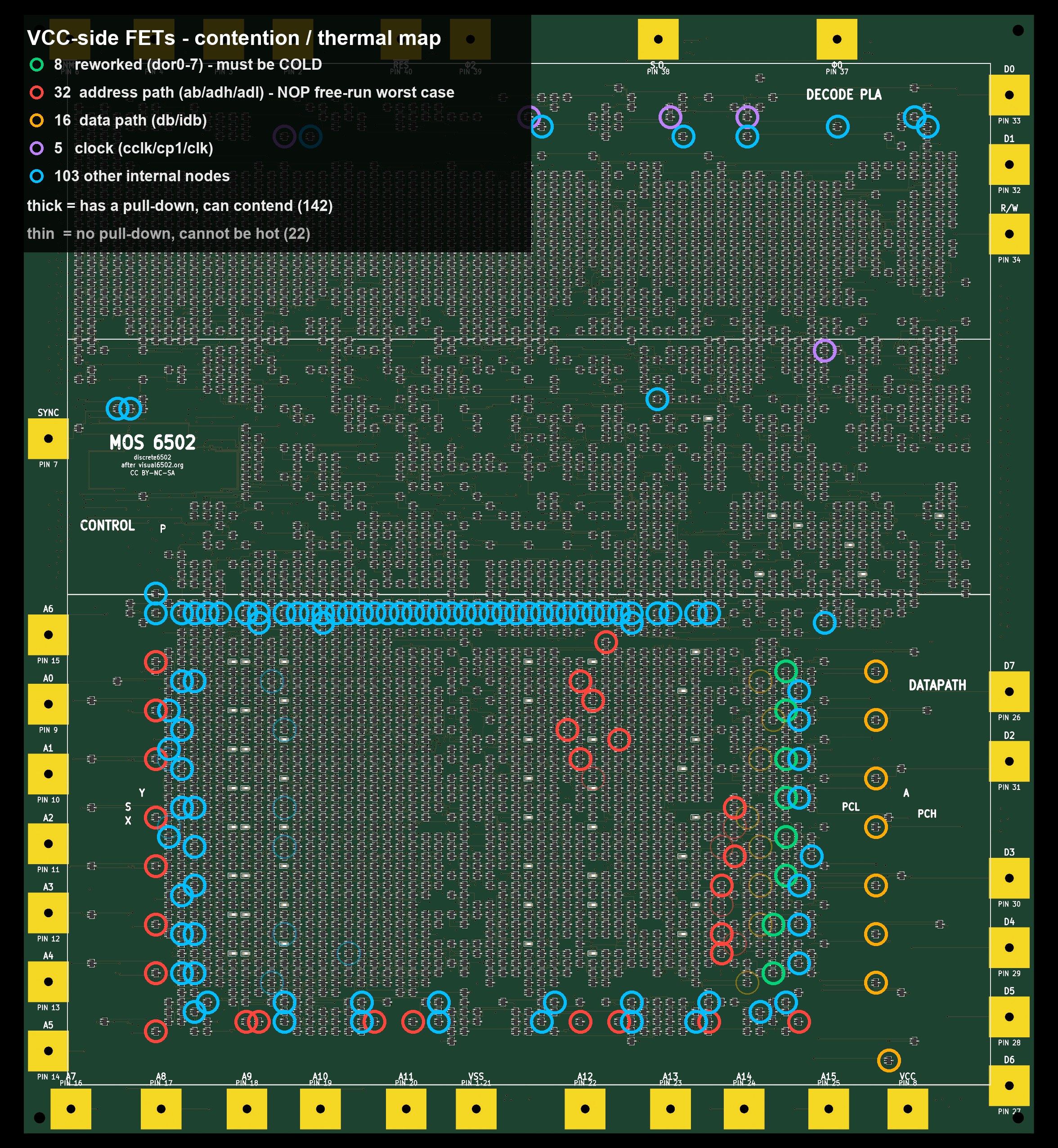
tools/mark_hotsites.py generates the site map used
for the sweep: all 164 VCC-side FETs on the top-face render, grouped by what they drive, with the 8
reworked sites and the 22 that have no pull-down and therefore cannot be hot marked
distinctly. The 142 that can contend independently reproduces the plan's rev B site count.
Gate: no site above ~30 °C, under this workload. SCOPE CORRECTED 2026-08-25 — see Step 5/6. The observation stands and the conclusion drawn from it does not: this image was taken during a NOP free-run, and the sites that run at 80 °C under real code contend 0.3% of the time under NOPs. Concentrated contention is real; it was not being exercised here. What this image does prove is that the Step 4 rework works — the dor eight contend 91.8% of the time in exactly this condition and are cold.
PASSStep 3c — The CPU executes, 2026-08-25
The program counter is counting. After rewiring the supply, tying irq
and nmi high and halving the clock to 2250 Hz, a 14.7 s clip of the register LEDs
contains the 6502's program counter, bit by bit, at exactly the frequencies arithmetic demands.
This board is a working CPU.
The test, and why it needs no LED to be identified
On a NOP free-run the CPU does nothing but fetch and increment, so the PC is a pure binary counter
and every PCL/PCH LED must blink at a rate fixed by the clock alone:
instructions/s = clock / 2        (NOP is 2 cycles)  = 1125
PC bit b toggles at  1125 / 2^(b+1)
Either those frequencies are present or they are not. No LED has to be located, named or mapped.
What makes it conclusive: named bits in a measured ladder
Corrected later the same day. This section first argued that the aliased
fast bits were the decisive evidence — that PCL4's 35.2 Hz folding to 5.256 Hz was a number nothing
else could produce. That argument is wrong. Aliasing requires point sampling, and a
camera integrates over its exposure, which low-passes the signal: a 562 Hz LED averaged over
even a 1/500 s exposure spans ~1.1 cycles and comes out a constant glow. PCL0–PCL5 are physically
unmeasurable from video, and the apparent detections at their aliased frequencies were drift
artifacts — the board wanders 76 px through this clip, which manufactures spurious
blobs and modulations in a max projection. Named-LED analysis
(tools/led_picker.py + --labels) falsified it. The conclusion stands on
better evidence instead.
The real proof is four LEDs identified by name, each measured against its own
predicted rate — a test that can fail, unlike the anonymous one:
LED
predicted
measured
error
SNR
PCL7
4.395 Hz
4.407 Hz
0.3%
13.9×
PCH0
2.197 Hz
2.170 Hz
1.3%
12.8×
PCH2
0.549 Hz
0.542 Hz
1.3%
10.2×
PCH3
0.275 Hz
0.271 Hz
1.3%
21.7×
And the ladder, on measured rates — each bit half the one above:
PCL7 -> PCH0   measured ratio 2.031, expected 2.000  ok
PCH0 -> PCH2   measured ratio 4.000, expected 4.000  ok   (PCH1 unconfirmed)
PCH2 -> PCH3   measured ratio 2.000, expected 2.000  ok
The remaining eight marked bits all reported the same 0.475 Hz — one artifact,
not eight signals. Their markers sit on genuinely lit LEDs (peak redness 186–202, duty 0.22–0.58),
so it is not misplacement; 0.475 Hz is a 2.1 s period, i.e. camera sway showing through as residual
tracking error. Where a bit has a real visible signal it dominates; where it does not, the residual
wins. PCL6 at 8.789 Hz is below Nyquist and should have worked — that it did not is
unresolved.
Two traps that caused four sessions of false negatives
Recorded because both are easy to repeat, and both produced confident wrong answers:
Aggregating across LEDs. Only 16 of the 55 register LEDs are PC bits, so averaging
spectra over everything visible buries them under the other 39. Count LEDs whose own dominant
peak matches instead.
The record's own envelope. A run that starts and stops inside the clip puts a large
peak at 1/duration, which impersonates a low-frequency PC bit — it faked a 0.55 Hz "signal" at 11.9×
the noise floor on 2026-08-24. Detrend each series with a cubic first.
Underlying both: only the direct low-frequency bits were ever looked for, and those
live in the same part of the spectrum as every slow artifact. Naming the LEDs, not chasing aliases,
is what made the test falsifiable.
What it proves, and what it does not
Proved: the board fetches, decodes and executes, and the PC increments correctly through at
least 12 bits. That requires the decode PLA, the PC incrementer, the address drivers and the
on-board clock phase generation to all be working — 4,051 discrete transistors doing 6502 logic.
Not proved: a NOP free-run never touches the ALU, A/X/Y, the stack, the flags, addressing modes or
branches. Klaus Dormann's suite remains the acceptance gate.
It also retroactively confirms several things at once — the clock regenerates on-board, the dynamic
nodes hold charge at the leakage measured in Step 2b, the rewired supply holds, and the
irq/nmi pull-ups took (a spurious interrupt would vector PC to $EAEA and
destroy exactly this ripple).
Gate: PC bits present at their predicted frequencies, four of them identified by name
and forming a measured factor-of-two ladder, with no unexplained peaks. PASS.
PASSStep 5/6 — The Pico is on, and the CPU runs a real program, 2026-08-25
The A register is counting, driven entirely by the board's own Pico. Until now every
clocked run used an external Arduino and a resistor tie-off. This is the first time the 6502 has
fetched from emulated memory, executed, and written back — the design working as designed.
discrete6502 running from Pico — the A register counting,
clocked and fed by the board's own Pico 2 W.
(watch on YouTube)
Module soldered to the underside site, pin 39 included, resistance re-checked the range-aware way
before power. Autorun on, so it began clocking the moment the rail came up. The built-in counter image
runs and the A LEDs count.
But it draws 2.3 A, and that reopens a closed question
Expected 0.7–1.2 A. Three independent observations say why, and together they reverse the
correction made in Step 3b.
The current is the same at 500 Hz as at 10 kHz. This is the decisive one and it
needs no model. Switching loss and near-threshold conduction both scale with clock rate. A
cclk-gated contending pair conducts a fixed fraction of every cycle and does
not. A 20× change in clock producing no change in current is what static contention looks like and
nothing else does.
The FLIR shows discrete spots at ~80 °C — precisely what Step 3b recorded as
absent.
The duty cycle was measured, not assumed, by a new tool.
Why both thermal images were right
tools/contention_duty.py measures how often each of the 164 VCC-side FETs is fighting
its pull-down. switchsim cannot see this — _value() returns low the moment
vss joins the conduction group, so it assumes the pull-down wins, which is exactly how the
1:1-ratio defect passed five green gates. The same model still exposes contention, just not through
the value: the VCC-side device is on and the group reaches vss.
Run under two workloads, it reconciles the two images completely:
CORRECTED 2026-08-26. This section originally read the table above as showing
that adh1/3/5/6/7 contend 35% of the time under real code and 0.3% under an all-NOP
free-run, and concluded that the Step 3b image was sound but its generalisation was not, because it
had been taken during a NOP free-run. The 0.3% was an artifact and the reconciliation is
dead. The measurement ran 150 cycles, during which the program counter barely moves, so PCH
sat at $EA throughout — and adhis the high byte of the
address during a fetch. The bits that read 0% were exactly the bits set in
$EA: a bit already high is not being pulled low and cannot contend. Re-run with PCH =
$00 and all eight read 48%. Contention here is address-dependent, not
workload-dependent; over any real run the address sweeps and every bit spends about half
its time low. Why the Step 3b sweep found nothing is therefore unexplained again,
and is recorded as open rather than papered over.
The strongest positive result: the Step 4 hand rework demonstrably works. The eight
dor nets contend 91.8% of the time under NOP free-run — right through the
whole Step 3b measurement — and the camera found them cold. Unreworked, that would
have been ~7 W in eight SOT-323 packages and impossible to miss.
The camera beat the model twice
First by finding the spots at all. Then by marking adl4–adl7 among the
hottest when the tool had excluded all four before measuring them. They have no
pull-down FET sitting directly between the net and vss — but they are pulled low through a
pass-gate chain, which contends identically. The FETs the filter did find on those nets are
gated by adl4–7, i.e. loads those nets drive: the same "counted FETs gated by X rather than on
X" error already recorded against cclk on 2026-08-01, repeated. Removing the filter
promoted adl6 and adl7 to 45.7%, the two busiest sites on the board, above every
adh and every dor.
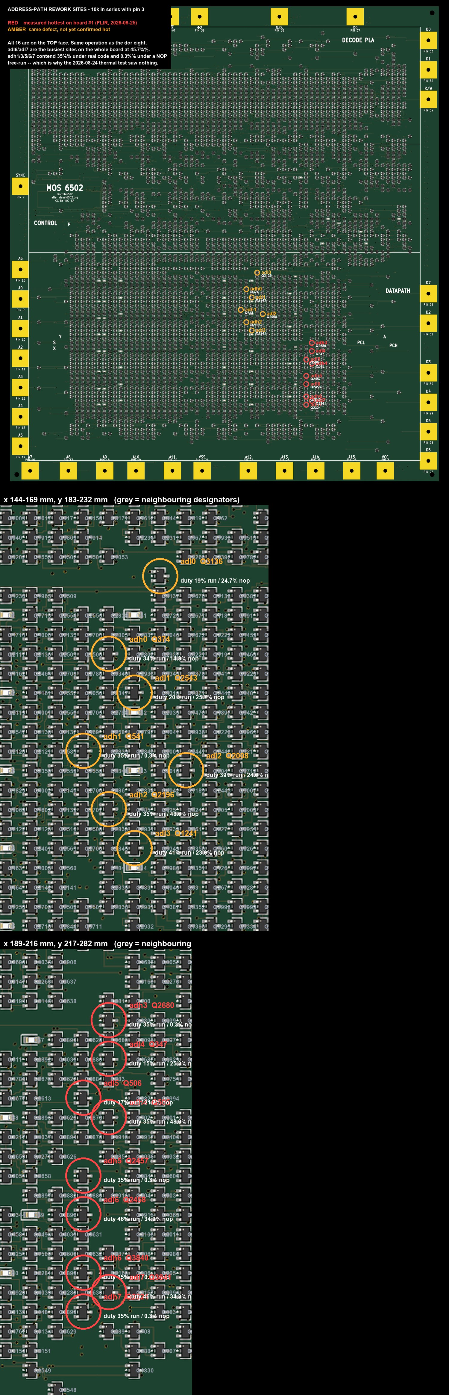
Why one cluster runs hotter than the other, at nearly the same duty
Heat was reported at both groups but much more at the lower-right one. Per-part duty differs by only
11%, so the difference is layout, and it is quantified rather than asserted:
            sites  mean duty  x-spread  mean NN  duty/cm2  neighbour-duty <12mm
panel 1       7      31.9%     14.8 mm   8.8 mm    20.7          36.4%
panel 2       9      35.4%      3.7 mm   5.1 mm    54.5         102.7%
Panel 2 packs nine sites into a 3.7 mm-wide column: 2.6× the dissipation per cm² and 2.8×
the neighbouring dissipation. Same watts per part, much hotter neighbourhood. Fixing panel 2
first should gain more than the sum of its parts, because it removes the mutual heating too.
The rework list, and what is not on it
Sixteen address-path sites want the same 10 kΩ-in-series fix (8 adh,
8 adl); nine are confirmed hot. Positions, designators and neighbouring parts:
rework-adh-marked.jpg.
The 16 ab* output drivers measure 0.0% under both workloads and are cold on the
camera. They do not want reworking, despite being flagged as "NOP free-run worst case" on the
older hotsites-marked.jpg.
Two observations still unresolved
The ammeter wanders 1.9–2.8 A on a cheap meter. A 0.9 A swing is hard to explain
from the board — under NOPs the CPU does the same thing every cycle, so the contended set should be
more constant, not less. Suspects are contact resistance in the croc path (~0.33 Ω per
segment at 2 A, already flagged on 2026-08-24) and the meter itself, which produced a badly wrong
reading once before. Next check: watch TP36/TP35 voltage and the current together — if they move in
step it is the wiring.
The board sings. An audible tone tracking the clock, obvious at 10 kHz and gone at
20 kHz — almost certainly because 20 kHz is past the listener's hearing, not because it stopped. Cause
is MLCC piezoelectricity: Class II ceramics deform under applied voltage, and this board carries 96 ×
100 nF and 4 × 10 µF on a 291 × 322 mm soundboard. For them to sing the rail must be rippling
at the clock rate, which corroborates the supply-path suspicion above: the precharge pulse
moves ~90 nC per edge, and through 0.5–2 Ω of lead resistance that is 45–180 mV of ripple. It also
gives a free confirmation test — adding bulk capacitance or shortening the supply path should make it
quieter.
Gate: the CPU executes a real program from emulated memory. PASS.
Current is 2× budget from address-path contention, which is understood, located, and fixable by an
operation already proven on this board. Do not start the multi-hour functional test until the
rework is done — 80 °C is over the SOT-323 power rating, though junction is ~90–110 °C
against a 150 °C limit, so short runs are fine.
CorrectionStep 6b — The NOP test, and the prediction it broke, 2026-08-26
Every adh site ran hot under NOPs, and the prediction said four of them would go cold.
The board was right and the model was wrong.
The test was meant to be decisive: load gen/nopfill.hex (16 KB of $EA), re-shoot the
same column, and watch adh3/5/6/7 go cold while adh4 got hotter. Instead
they all stayed hot — but the run produced a better result than the prediction would have.
Why the prediction was wrong
tools/contention_duty.py ran 300 half-cycles. The program counter barely moves in
150 cycles, so PCH sat at $EA for the whole simulation — and
adhis PCH during a fetch. A bit that is already high is not being pulled low,
so it cannot contend. Re-run the identical measurement with the reset vector changed:
The bits that measured quiet are exactly the bits set in $EA
— 1, 3, 5, 6, 7. Contention here is address-dependent, not workload-dependent.
Over a real run the address sweeps, every bit spends about half its time low, and all of them heat.
What the board showed instead, which is stronger
Watching the image, adh6 and adh7 were seen to stay cold about a second
longer than the others and then heat up as well — cycling, not merely warm.
That is quantitative. PCH increments every 256 instructions and bit n toggles every
2n of those, so at 10 kHz (NOP = 2 cycles, 5,000 instructions/s):
T = 2^n x 512 / f_clock

adh0..adh4   50 ms .. 0.8 s     faster than the copper's thermal time constant
adh5         1.6 s
adh6         3.3 s              <- observed cycling
adh7         6.6 s              <- observed cycling
The only two bits slow enough for thermal mass to follow are exactly the two that were seen
cycling. This is the program-counter ripple measurement of Step 3c again, in the thermal domain
instead of the optical one, and it is a stronger confirmation of the contention mechanism than the
prediction it replaced. A worthwhile follow-up before the rework removes it: film
30 s of FLIR and check adh7's period is exactly twice adh6's.
What it changes
All sixteen sites want the rework, and the "some are only hot under real code"
nuance is gone — it was never real.
Why Step 3b saw no hot spots is open again. The workload explanation was the
only thing reconciling it, and it is dead. Same board, also a NOP free-run, address also sweeping.
No replacement explanation is offered here, because none has been earned.
The measurement tool now carries a caveat and its low readings are labelled
"quiet at THIS address". A duty gate for rev B must sweep addresses or it will certify sites that
contend heavily in use.
Gate: the prediction failed and the mechanism survived. Rework all sixteen.
PASSStep 6c — What the board actually draws, 2026-08-26
Clock stopped: 0.30 A. Executing: 1.70 A. The stopped figure is the passive network
behaving exactly as designed. The 1.40 A difference is contention, and it is now a number rather
than an inference.
The stopped current settles a question that has been open since Step 2
Step 2 measured 1.4 A unclocked against a 0.35 A prediction and that gap drove a
fortnight of reasoning. It was measured with no Pico on the board — so
clk0, which has no pull-up on this board, along with the data bus and reset, were all
floating. That condition genuinely does let the dynamic nodes drift to undefined levels and
bias thousands of FETs near threshold, which is what the Step 3b correction proposed.
It is not the condition the board runs in. With the Pico fitted and the clock
parked at a defined level, board #1 draws 0.30 A — against a design prediction of
0.35 A typical and a passive ceiling of 0.548 A. Nothing is wrong with the board at rest, and never
was.
The running current, and what it says per net
stopped     0.30 A     passive network, as designed
executing   1.70 A     mean over 30 s (range 1.05 - 2.40)
            ------
contention  1.40 A
Against switchsim's ~7.7 nets contended on average on this board, that is about
180 mA per contended net — the same quantity sim/driver_contention.sp
puts at 262 mA for a worst-case gate drive. Two independent routes to the same number, sim on the
high side as expected.
Two smaller results from the same session
Power-on order matters, by about 0.65 A. Hot-plugging the VCC croc onto an
already-live charger gave a mean of ~2.35 A; connecting both clips cold and then energising at the
charger gives 1.70 A. Keep the second ritual — it is better practice regardless,
since hot-plugging a 2 A load onto a crocodile clip arcs and pits the contact.
The fluctuation is the CPU, not the instrument. It had been treated as a meter
or contact problem for two days. With the clock stopped the reading is steady, so whatever moves it
is the processor. A 30 s recording of the meter was OCR'd and tested for the period the address
counter would produce — no support (r = +0.02 at 6.5 s, −0.10 at 13.1 s, against a
±0.09 noise floor). The magnitude fits (a 1.35 A swing at 180 mA/net is about 7 nets moving in and
out, the right size for the address bits sweeping) but the periodicity does not, and 30 s is only
two cycles of the period being looked for. Recorded as unresolved.
Gate: a stopped board draws its designed passive current. PASS.
Target for the sixteen-site rework: the adh/adl sites are about 5.2 of the
7.7 nets contending, so executing current should fall from 1.70 A to roughly
0.7–0.9 A, with the stopped figure unchanged at 0.30 A.
Reproducing the analysis
The numbers on this page are generated, not asserted:
python3 tools/pc_ripple.py --clock 2250 --frames FRAMES/   # Step 3c: find the PC
python3 tools/contention_duty.py                          # Step 6: contention duty
python3 tools/mark_rework_adh.py                          # Step 6: the rework map
python3 tools/make_nop_image.py                           # Step 6b: the NOP image
python3 tools/step1_model.py      # Step 1: the body-diode model and the meter readings
python3 tools/dynamic_nodes.py    # Step 2b: retention, the 456 dynamic nodes, the clock window
python3 tools/mark_hotsites.py    # Step 3b: the 164 VCC-side FETs on the board render
It reads gen/netlist.json, proves there is no resistor-only path between the rails,
counts the body-diode branches, predicts the display against test current, inverts the measured
readings, and computes the reverse-direction slope. The measured values are recorded in the
MEASURED table at the top of that file, so adding a board or a range means editing one
list.
Authoritative sources, in order of precedence when they disagree:
pico-controller/README.md for the sequence and the firmware,
project-plan.md for the measurements and the risk picture,
the rework page for the eight sites, and
gen/board_routed_golden.kicad_pcb for anything geometric.