discrete6502 — the bring-up sequence for the boards as delivered: 4 assembled,
1 bare. Sources: pico-controller/README.md (the authoritative sequence),
“Driver contention” and “Expected fab yield” in project-plan.md, and
the rev A rework page. What actually happened when these steps were run on the real boards is logged separately:
bring-up as it actually happened.
Read this before you connect anything.
Use a bench supply with an adjustable current limit. Never USB, and never a
charger. The current limit is what protects a mis-assembled board — not a lower
rail voltage, not luck. A charger will happily push 3 A into a partially-conducting
driver.
Size the supply for 3 A, not 1 A. The clocked board draws
≈2.1 A until the rework is done, and ≈0.3 A after it.
ESD precautions throughout. 4,051 MOSFET gates sit on dynamic nodes with
no protection whatsoever. Wrist strap, mat, handle by the edges.
Do not run the retention test (w / W) before the
rework. Freezing the clock is precisely the condition that parks a pull-up and a
pull-down on together. Before the rework that is 262 mA and ~0.9 W per site; after
it, 0.5 mA.
Bring up one board at a time. You have four. Take one all the way through
and leave the other three untouched until you know what a good board looks like.
The sequence at a glance
Why the rework sits at Step 4 and not earlier or later. Steps 1–3 are the only
tests that can detect a systematic assembly fault — a wrong reel, a bridged rail, a
rotation error — and all of them would make the rework wasted labour on four boards. Everything
from Step 6 onward involves sustained clocking, which is the condition that makes the defect
thermal. So the rework goes exactly between them.
Numbering, reconciled.pico-controller/README.md carries the same
sequence under its own numbering, which predates this page and is referenced from elsewhere in the
repo. The steps map like this: this page's Steps 0–2 are its Steps 1–2, Step 3 is the
optional paragraph at the end of its Step 2, Step 4 is its Step 2b,
Step 5 is its Step 3, and Steps 6–8 are its Step 4. Same order, same gates.
What you need
Instruments
Bench supply, 3 A, adjustable current limit and a readable current
display. The display is an instrument here, not a convenience — several steps below are
nothing but reading it.
Multimeter with fine, sharp probe tips. Blunt probes slip onto neighbouring
parts on a board this dense.
Croc-clip leads. The 11.6 mm bond pads exist precisely so croc clips
work from the back.
Optional but valuable: a function generator (Step 3) and an oscilloscope.
For the rework (Step 4)
8 × 10 kΩ 0603 resistors, plus spares — buy 20–25. 0.1 W is the
standard 0603 rating and is 40× what these dissipate (~2.5 mW). Tolerance is
irrelevant; this is a load, not a divider. 0402 (the board's own size, LCSC C25744) also
works but is fiddlier for this method.
Fine-tip iron (1 mm conical or bevel), fine solder (0.3–0.5 mm, leaded if you have
it), tacky flux, fine bent tweezers, solder wick, magnification, IPA and a brush.
30 AWG wire-wrap wire for the optional leg-to-resistor link.
Kapton tape, and a flat support for the board.
For the Pico (Step 5)
A Raspberry Pi Pico 2 W, SMD-mount variant. The site is DNP — the boards
arrive with no Pico on them.
A USB cable for flashing and serial.
Software
pico-sdk 2.x and arm-none-eabi-gcc, to build pico-controller/tester
(and later wifi). Build with PICO_BOARD=pico2_w.
A serial terminal.
For Step 8: Klaus Dormann's 6502_65C02_functional_tests, assembled to Intel hex.
No powerStep 0 — Receiving inspection
Before a probe touches anything.
Put the ESD strap on first, and work on a mat. Handle every board by its
edges.
Photograph the packaging before you open it, and each board as it comes out.
If there is shipping damage, this is your evidence. A 300 × 322 mm 6-layer
board is a plausible flex casualty in transit.
Support each board flat. 1.6 mm thick over a 300 mm span is a
floppy ratio, and the underside is populated with passives — support it on something soft
and full-area, never clamped by two edges.
Visual inspection of all five. Look for tombstoned passives, solder bridges,
missing parts, and — most valuable — sweep your eye down the FET field checking that every
SOT-323 pin-1 marker is in the same corner. Rotation was already verified on
JLC's DFM image before production, so this is confirmation rather than discovery, but it is
the one fault that takes out all four boards at once.
The bare board will probably still carry its two 5 mm edge rails, since
depaneling is a PCBA-side option. Snapping those off an unpopulated board by hand is safe.
Do not flex the four assembled ones.
Set the bare board aside. Its job is to be looked at and to be a reference
artefact — it is the die artwork with nothing in the way. It is also your spare.
Expectation setting, so a defect does not read as a disaster. The pre-arrival
estimate in project-plan.md is 0.5–2 defects per board across ~14,700
solder joints. Expect 2 of the 4 to work at first power-up (plausibly 1–3), ~85%
odds that at least one does, and 3–4 working after rework. A single-defect board is a repair job,
not a loss: every FET is on the top face, and the functional test localises failures to a block.
The one pattern worth noticing is clustering — thermal mass and warpage on a board this
large make defects more likely to group by region than to scatter. If failures map onto one area of
the die, suspect the reflow profile, not a random joint.
No powerStep 1 — VCC↔VSS resistance
Measure resistance from a VCC bond pad to a VSS bond pad on each of the four
assembled boards. Record the polarity and the range with every number — on this
board a bare figure in ohms is meaningless, for the reason below.
Gate: red on VSS reads a few hundred ohms and the value changes with range;
red on VCC reads OL on a low range.
This gate used to say “it must read high”, and that was wrong. It is left here as a
correction rather than quietly fixed, because it made a healthy board's first measurement look like
a fault. Measured on the real boards: ≈195 Ω on the 200 Ω range with the red probe on
VSS, on all four. See
bring-up as it actually happened for the full dataset and the
analysis.
There is no resistive path between the rails at all — verified against
gen/netlist.json by tools/step1_model.py. The meter is reading a
junction: every pull-down FET's body diode conducts VSS → drain, and where that drain
carries a 10 kΩ pull-up it forms a VSS → VCC branch. There are 1,899 such body diodes
across 947 nets. So what the meter displays is a diode drop divided by whatever current
the selected range happens to source, and it legitimately reads 195 Ω, 314 Ω or 3.77 kΩ for the
same board.
What identifies a genuine fault is therefore not a low number, but a number that behaves like a
resistance:
Under ~1 Ω — a solder bridge. The rails are solid planes with thousands of
stitching vias; a bridge reads a fraction of an ohm, not hundreds.
The same value on every range, in both polarities — a real resistive path.
A junction cannot do this; its apparent resistance must move with range.
One board unlike the other three.
Record all four numbers. The absolute value matters less than the comparison: four
boards from one panel and one reflow should agree closely. The odd one out is telling you something
before you have spent any current finding out.
This step proves more than the absence of a bridge. The forward path only exists
if the 10 kΩ pull-ups are populated — without them there is no route from the body diodes to VCC
and the board reads open both ways. A forward reading in the expected band is positive evidence
that the back-side pull-up network and the FET array are present and connected, which is not
something you can confirm by eye on 0402 parts.
5 VStep 2 — Board alone at 5 V, unclocked, no Pico
This is the single most informative measurement in the whole project. It finds a
bridged rail, a reel loaded backwards, and missing pull-ups — the faults that would otherwise be
identical on all four boards.
Procedure
Croc-clip the supply to a VCC bond pad and a VSS bond pad.
Set the current limit to 0.5 A and the voltage to 5 V.
Ramp the voltage up from zero while watching the current, rather than
switching 5 V on in one step.
Read the current at 5 V.
What the number means
Reading at 5 V
Verdict
≈0.35 A
The prediction. This is a healthy board.
Up to 0.65 A
Still within the legitimate worst case — every pull-up low and
every LED lit. Unusual but not a fault.
Folds back into current limit at near-zero volts
A short. Stop, find it.
Folds back only near 5 V
Ambiguous — see the box below.
Grossly high, or grossly low
A systematic fault: bridged rail, wrong or backwards
reel, missing pull-ups. Do not proceed, and do not rework three more boards.
A tension in the numbers you should know about before you meet it. The documented
worst case for a healthy unclocked board is 0.65 A, but the recommended limit is
0.5 A — so a legitimate worst case would trip the limit and be indistinguishable from a fault.
That is why you ramp: where it folds back is the diagnostic. A bridge limits almost
immediately, at a fraction of a volt. A healthy-but-high board limits near the top. If it limits
near the top and you need to distinguish the two, raise the limit to 0.8 A —
still far below the ~1.8 A that driver contention would draw, so the limit stays diagnostic
rather than merely permissive.
An honest caveat on “unclocked means no contention”. The reasoning is that
contention needs live logic state and an unclocked board has none. That is likely but not
guaranteed: on an unclocked board the dynamic nodes are not in a defined state, they float at
whatever power-up charge leaves them, and nothing forbids a dor bit's gate and its
pull-down's gate from both sitting above threshold. The claim is really “sustained contention is
unlikely without clocking”, not “contention is impossible”. It does not change what you do, because
the protection was never the absence of contention — it is the current limit. At
0.5 A the supply folds back the moment two nets contend at 262 mA each, the rail sags, and
dissipation stays far below the level that damages a SOT-323. These parts fail from sustained
heating, which a current-limited supply prevents.
Gate: a current reading you understand, on a board you are willing to keep.
5 VStep 3 — Optional: an external clock, and watch the LEDs
Worth doing. It is the first evidence that the logic itself lives, and it needs no firmware.
Croc-clip a function generator to the Φ0 bond pad.
Drive clk0 push-pull at a few kHz. The board has no pull-up on
clk0 — an open-drain driver would leave it floating, and a dynamic CPU cannot survive
that.
Watch the register LEDs.
The data bus floats, because no memory is connected, so the CPU executes garbage. That is fine
and expected. What matters is that the register LEDs move. Movement proves two
things at once: the internal clock phases (cclk, 482 gates; cp1, 198
gates) are being regenerated on-board at full VCC swing, and the dynamic logic is holding charge
between edges.
Corrected 2026-08-24, from measurement. This block used to say "seconds, not
minutes", and to expect the current to jump toward ~2 A when the clock started. Both
were wrong, and in opposite directions. Measured on board #1: the board draws
1.4 A unclocked and clocking brings it down to 0.7–1.2 A, so the
expected change is a fall, not a jump. And FLIR imaging found no hot spot
anywhere — peak ~30 °C against 25 °C ambient — because the excess current is
spread over thousands of near-threshold FETs rather than concentrated in a few contending pairs. The
board is not being damaged and can be run as long as a measurement needs. Keep a current limit on if
you have one, but the urgency was an error. See
the measurement log, Steps 2 and 3b.
Doing it with an Arduino instead of a function generator
A 5 V Uno or Nano is a good fit, for one specific reason: its outputs are push-pull.
That is not a convenience here — clk0 has no pull-up on the board (only
R1079, 100 R, and the clamp diodes D66/D67), so an
open-drain or tri-stated driver would leave the clock floating, and a dynamic CPU cannot survive
that.
Arduino
Board
Why
D9
Φ0 bond pad
The clock. Goes through the on-board
100 R; no external pull-up needed with a push-pull driver.
GND
VSS bond pad
Mandatory. Without a common reference
nothing works, and the clock edge is undefined.
D8
RES bond pad
Or croc-clip straight to VCC. RES has
no pull-up — only R1074 and its clamps — so it must be driven.
—
IRQ, NMI → VCC
Both float: 100 R
and clamp diodes only, no pull-up. A floating gate on a dynamic input can drift across
threshold and fire a spurious interrupt.
—
RDY, SO — leave alone
These two do carry 10 k pull-ups
(R48, R991).
Do not power the board from the Arduino. The board draws
1.4 A unclocked and 0.7–1.2 A clocked (measured, board #1) — far past
what the Uno's regulator can supply and well past USB-only sanity. Bench supply for the board, USB
for the Arduino, grounds commoned through the table above.
void setup() {
  pinMode(8, OUTPUT); digitalWrite(8, LOW);   // RES asserted low
  tone(9, 4500);                              // clock running FIRST
  delay(20);                                  // ~90 clocks at 4.5 kHz
  digitalWrite(8, HIGH);                      // release reset
}
void loop() {}                                // tone() is timer-driven
4–5 kHz is the frequency to pick. This used to say 1–2 kHz, against a
predicted retention floor of ~378 Hz; the floor has since been
measured at 456–871 Hz (leakage 1.9–2.3 nA
per FET), which left 2 kHz only 2.3× clear of it. The usable window is [871 Hz,
20 kHz] and its geometric centre is 4.2 kHz — 4.8× clear of the floor and
4.8× below the fanout ceiling. Jitter is irrelevant — dynamic logic cares only about the maximum
period, not about stability — so tone() is entirely adequate and no timer configuration
is needed.
Tie the data bus off, or the CPU will jam. With it floating the CPU fetches
random opcodes, and 12 of the 256 are undocumented KIL/JAM — a 4.7% chance per fetch,
so it halts within ~20 instructions and the register LEDs simply decay to a frozen state. Tie the bus
to $EA (NOP) through 10 kΩ — db1, db3, db5, db6, db7 high to VCC,
db0, db2, db4 low to VSS — and it free-runs the whole address space instead. Resistors,
never wires, so the CPU wins if it ever drives the bus. Locate those pads
by silk label, never by counting: four rev A pads sit in the wrong slot
(cards/bond-pad-ring.md).
Tying RES straight to VCC is enough for a smoke test, but the sequence above gives the CPU a
defined entry: clock first, then release reset. Note the ordering. Releasing reset into a stopped
clock is the stall condition.
The one rule: never stop the clock while the board is powered. Kill
the supply first, then the Arduino. A parked clock is what freezes the dynamic nodes and parks a
pull-up and pull-down on together.
No powerStep 4 — The eight-site 10 kΩ rework
Full illustrated instructions, with true-scale renders of all eight sites and their
neighbouring designators: the rev A rework page.
Follow that page for the procedure; this is only why it belongs here in the sequence.
The board as fabricated has a device-ratio defect: the eight data-bus output drivers use a
BSS138W as the load against a BSS138W as the pull-down — a 1:1 ratio where ratioed NMOS needs a
weak load. Measured consequences at 5 V, per contended site:
As built
With the 10 kΩ
Contention current
262 mA
0.499 mA
The contended “low”
1.86 V — invalid
2.9 mV — valid
Dissipation in the pull-up FET
0.90 W in a SOT-323 rated ~0.3 W
2.5 mW
Board total, clocked
≈2.1 A / ≈10.4 W
≈0.3 A
The thermal problem is the loud one, but the functional problem is the serious one: a contended
node sits at 1.0–1.9 V against a 1.1–1.5 V receiver threshold, so the CPU can
write wrong data. The fix is simulated end-to-end in sim/revb_driver.sp, two
stages deep to a real chip output — it costs nothing in speed (271 ns rise against a
25 µs budget) and it makes the output level higher, not lower.
Eight sites, all on the front face, in one column at x ≈ 220 mm (dor6/dor7
at x ≈ 216.5 mm), 11–14 mm apart. Same part, same orientation, identical copper — it is
the same operation eight times.
Confirm each part against the table on the rework page before you touch it. Every
neighbour is an identical SOT-323. This is the step where the wrong transistor gets reworked.
Gate, per site: pin 3 lead to a VCC bond pad reads 10 kΩ; pad 3 to VCC
still reads ~0 Ω.
Gate, whole board: VCC to VSS still reads high — you have not introduced a bridge.
Clean the flux off after each site and inspect under magnification. Then repeat Step 1 and Step 2
on the reworked board; Step 2 should be essentially unchanged, since contention was near zero
unclocked anyway.
If you would rather not rework: the alternatives are running at 3.3 V (halves
the current but leaves the low level invalid — a mitigation, not a fix) or accepting eight FETs at
~0.9 W and expecting them to fail. Neither is viable for the functional test. See “Rework
options” in project-plan.md.
No powerStep 5 — Solder the Pico
Flash the tester firmware onto the bare module first, on the
bench, and confirm it enumerates over USB. Reasons below.
Solder the Pico 2 W module onto the underside site.
Solder pin 39. This is not a decision to be made per board.
Repeat the Step 1 resistance measurement.
Only then apply power.
Why flash it before soldering, when it can be reflashed in place
It can be reprogrammed in place, indefinitely and without touching the button:
pico_stdio_usb/reset_interface.c is linked into all three firmwares, so the SDK's
1200-baud-touch reset-to-bootloader works and picotool can reboot the module into its
bootloader over USB. Flashing once beforehand is still worth it:
You get to reject a bad module while rejecting it is still cheap. A dead or
damaged Pico soldered to this board is a miserable desolder job — the footprint's
3.2 × 1.6 mm pads run under the module — and you would be doing it
beside 4,051 transistors you care about. Two minutes on the bench buys that away.
The first flash is the one that needs BOOTSEL, held while power-cycling. That
is the awkward operation, and it is the one you can do off the board.
It makes the first power-up a known state rather than merely a harmless one.
A blank module is safe — RP2350 GPIOs default to inputs — but safe and known are not the same
thing.
The firmware is inert at boot, which is what makes pre-flashing safe rather than
presumptuous.main() calls bus_init(false) and then blocks on
while (!stdio_usb_connected()) sleep_ms(100);. A pre-programmed board powered up with no
terminal attached does nothing at all — no clocking, no reset ceremony. The CPU starts moving only
when you open a serial connection, which means the transition into Step 6 is something you choose
rather than something that happens to you.
One subtlety: bus_init leaves clk0 as an output driven LOW — every other
pin is an input. So a powered, pre-programmed board sits with the clock parked, which is the
stall condition: exactly what the retention test deliberately creates, and exactly what the
driver-contention defect makes dangerous. This is not a problem for the sequence as written, because
the Pico goes on at Step 5 and the rework happened at Step 4. It is a reason not to swap
those two steps, and a reason not to leave an un-reworked board sitting powered with a Pico fitted.
Check before you settle on a workholding setup: the module mounts pads-down, so its
component side — USB connector and BOOTSEL button — faces away from the PCB, i.e. downward
when the board lies flat on its back. You will want the board propped up or on standoffs to reach
the connector. This is reasoned from the footprint rather than from a board in hand, so confirm it
physically.
Pin 38 is vss and pin 39 is vcc, side by side on 2.54 mm
pitch. A bridge there is a dead short across the board supply. That is why Step 1 gets
repeated here.
Why pin 39 must be soldered rather than left off, which was considered and
rejected:
It removes the power-sequencing question entirely. Board VCC and Pico VSYS
become one node, so the hazard of a 5 V core driving 26 clamp diodes into a dead 3V3
rail becomes unreachable.
An unsoldered pin 39 is not an open circuit — it is an intermittent contact.
The footprint's 3.2 × 1.6 mm pads extend inward, under the module, so an
unsoldered castellation is two flat copper faces held apart only by whatever standoff the
neighbouring joints happen to give. Board flex or a croc clip closes it. A rail that makes and
breaks corrupts every dynamic node at once, and it reads as a random CPU fault.
With pin 39 soldered, either end can supply power: a bench supply on the bond
pads runs the board and feeds VSYS (connect USB for serial only), or USB into the Pico runs
everything through the module Schottky. Use the bench supply for anything that matters —
USB-only is not viable at 5 V now that the real clocked current is known.
5 VStep 6 — First clocked run: the A-register counter
This is the “it is alive” moment.
Build and flash the tester firmware
(pico-controller/tester, PICO_BOARD=pico2_w).
Power the board at 5 V from the bench supply, current limit at
1 A for this step. USB may stay connected for serial — the module
Schottky drops VBUS to ~4.7–4.8 V, so a 5.0 V bench supply wins the node and the
diode blocks back-feed into the host.
Open the serial terminal. Press h for the command list.
Run the default image — an A-register counter loop — and watch the A LEDs
count.
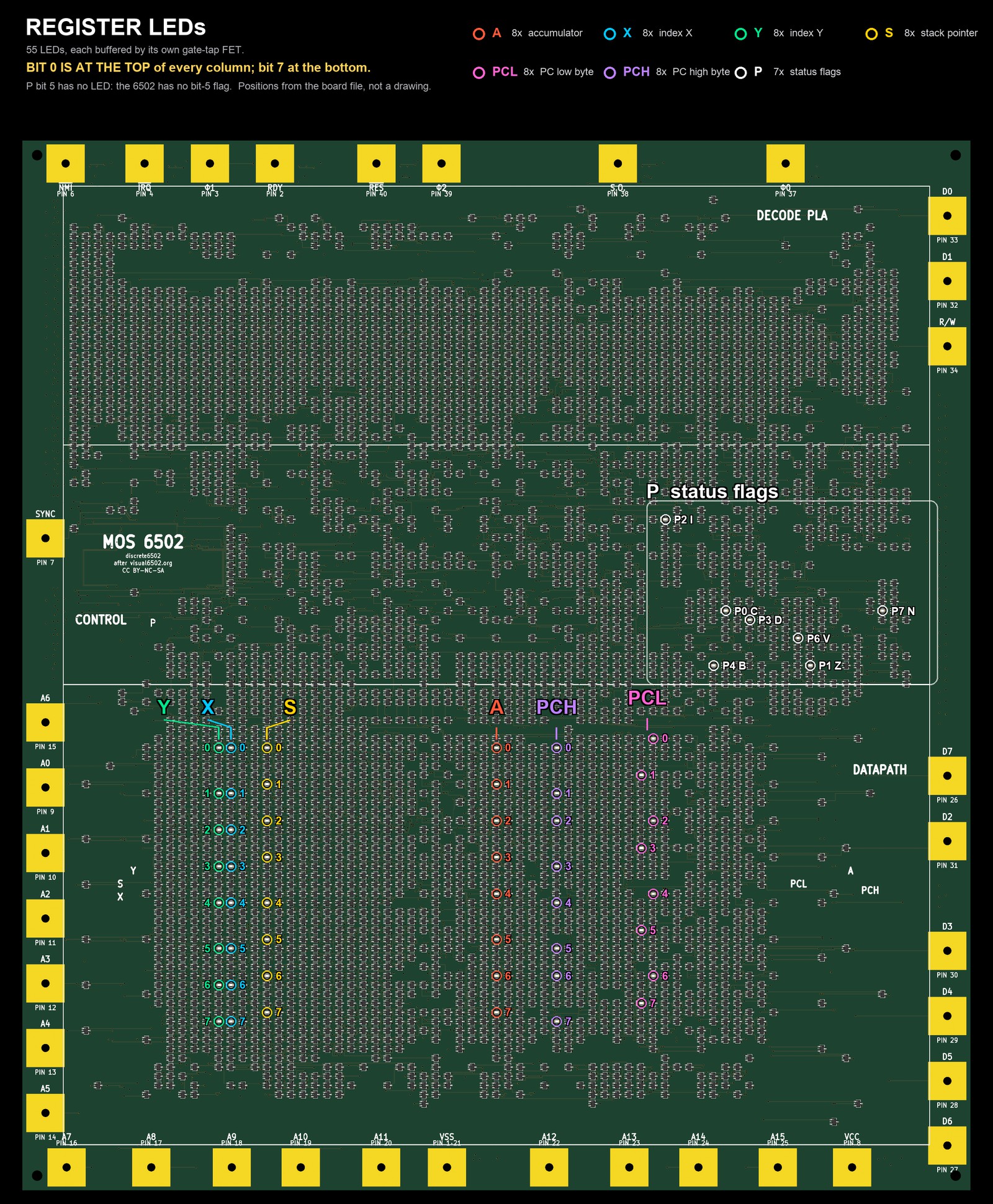
Which LED is which. Generated by tools/mark_leds.py from
gen/board_routed_golden.kicad_pcb and gen/netlist.json, so it matches
the board rather than a drawing — the tool verifies its own mm-to-pixel fit by checking that all
55 computed positions land on LED pad pixels before it draws anything. Click to enlarge.
Bit 0 is at the top of every column, bit 7 at the bottom. The six registers
are vertical columns in the datapath; Y and X are only 3.8 mm
apart, which is why their labels are splayed. The P flags are scattered across the
control block rather than in a column, so each is named individually
(P0 C, P1 Z, P2 I, P3 D, P4 B,
P6 V, P7 N) — and there is no P5 because the 6502 has no
bit-5 flag.
For this step the only LEDs that matter are the A column, at x ≈ 145
in the middle of the datapath. If they count and nothing else moves, that is exactly right: the
counter loop touches A and the PC, so expect the PCL column to be busy too.
The default clock is a 50 µs half-period, i.e. 10 kHz.
Watch the supply current
Gate: with the rework done, clocked current should stay in the low hundreds of mA.
If it jumps toward 1.8–2.1 A, a rework site did not take. That current step
is the measurement — it is the cheapest whole-board verification of the rework you will
get. Go back and re-check the eight sites.
Useful commands at this point
R          reset sequence (assert, 8 cycles, release)
c N        run N cycles (quiet)
t N        run N cycles, printing each bus cycle
s [N]      step N instructions, printing cycles
d [N]      dump the last N trace entries
x A L      hexdump L bytes of the image at offset A (hex)
m A B..    poke bytes at offset A (all hex)
z          zero the cycle counter and trace
If the LEDs do not count, t is the tool: it prints
cycle addr(14-bit) data r/W SYNC per cycle,
so you can see whether the CPU is fetching sensible addresses at all.
Remember the address space. The CPU exposes only 14 address bits to the Pico, so
memory is a 16 KB image mirrored across the 64 KB space. The reset vector
$FFFC/D appears at offset $3FFC/D.
5 VStep 7 — Measure the clock window
Two unknowns that only hardware can settle, and they are the two ends of the same window.
The ceiling — p
Walk the clock up with p US (half-period in µs) until the CPU stops executing
correctly. Simulation predicts ~20 kHz at 5 V (~10 kHz at
3.3 V), set by the decode-PLA input lines driving up to 71 gates behind a single 10 kΩ
pull-up. The M2 target was ≥50 kHz, so this is a known shortfall, not a surprise.
For scale: the original NMOS 6502's own specified window was 50 kHz to
1 MHz. A discrete rebuild of this logic style runs entirely below the band the real
chip was specified for, and the MOnSter's ~50 kHz ceiling sits on the original's
minimum.
The floor — W
Only after the rework. This is the test the safety rules exist for.
Dynamic logic has a lower clock bound as well as an upper one: stop too long and the stored
charge leaks away. w MS freezes the clock for MS milliseconds and asks whether the
state survived; W [MAXMS] finds the boundary by bisection, running a 0 ms control
first so a broken harness cannot masquerade as a result.
The worst nodes are sb1..sb7 — one gate of capacitance (32 pF) against
twelve FET channels leaking them. The big nets are the safe ones. The decisive number:
at the 20 kHz ceiling the worst node must leak under 53 nA per FET
(under 27 nA at 3.3 V), or the floor rises above the ceiling and there is no working clock
at all. Typical parts are ~1 nA, giving ~50× margin — but SPICE could not resolve leakage at
this level, so this is genuinely unmeasured until you measure it.
Start with sub-millisecond stalls and ramp up.
Keep the current limit on and watch the current through the stall.
The result also bounds how long the tester's single-step pause may safely last.
If you measured a floor before the rework as well, keep both numbers. A floor that
moves after the rework is evidence that the eight sites were heating their neighbours — leakage
roughly doubles every 10 °C, and eight drivers at ~0.9 W is a real thermal source. That is
worth knowing, and it is the only reason to have a pre-rework figure at all.
5 VStep 8 — The functional test: the acceptance gate
The bring-up acceptance target is Klaus Dormann's
6502_65C02_functional_tests — the standard suite for 6502
re-implementations rather than emulators.
Run the decimal test first
6502_decimal_test.a65 before the main suite. Decimal mode comes free from the
netlist and is the thing emulators most often get wrong, so it is a high-information, short test.
Build the images
Do not assemble by hand. tools/build_functest.py drives the suite's own assembler
and does the board-specific work — it needs a checkout of the suite as a sibling directory and
Docker, because AS65 1.42 is an i386 binary:
python3 tools/build_functest.py            # both tests
python3 tools/build_functest.py decimal    # just one
Outputs land in gen/functest/: a .hex ready for L, and a
_traps.csv listing every self-loop with its source line. The script sets
ram_top = $40 (the suite's own preset for a 16k mirrored system), folds
64 KB to 16 KB the way the hardware does and fails on a real aliasing collision,
patches the reset vector, and extracts the verdict map.
Both images have been executed before any hardware existed, and both reach PASS.
The toolchain first reproduces upstream's committed bin_files/6502_functional_test.bin
byte for byte, which validates the assembler path; then each generated image was run to completion
in an emulator against a mirrored 16 KB memory. The decimal test reaches its PASS loop in
46,089,513 cycles and the functional test reaches $34D8 in 96,779,996 cycles with
test_case at $F0. So a failure on the board is the board, not the image.
The addresses you need
Functional test
Decimal test
Entry
$0400
$0200
Progress address
$0200 (test_case)
$0001 (N2)
Progress range
0..43, then $F0 for the final phase
0..255, twice
PASS
$34D8
$024F
FAIL
any other self-loop — look it up in the CSV
$0252
Spurious NMI
$380B
$02F3
Spurious IRQ
$3819
$02F3
Cycles to PASS
96,779,996 — 2 h 41 m at 10 kHz
46,089,513 — 1 h 17 m at 10 kHz
Run it
p 50          # the conservative default clock
L             # paste gen/functest/<test>.hex into the terminal
k 0200        # watcher at the progress address ($0001 for the decimal test)
R             # reset
g             # go: run until a self-loop, printing progress
The reset vector is already patched in the image, so the old m 3FFC 00 04 step is no
longer needed.
How to read the verdict
The suite has no I/O, so the firmware reads two side channels off the bus: writes to the progress
address give live progress, and a repeated opcode-fetch address gives the verdict.
Pass and fail are both self-loops, distinguished only by address — which is why the
generated _traps.csv matters. It gives every failure address its source line and the
test_case number that was current, so a stop narrows 4,051 FETs to a functional
block.
Human-readable error messages are not available on this board — measured, not assumed.
The suite's report = 1 option prints text through an I/O channel, but it adds
3.5 kB and the image then ends at $466B, past the $3FFA ceiling of the
mirrored window. The two side channels are the whole story.
Tie irq and nmi high before a long run. Neither has a
pull-up on the board — only a 100R and the clamp diodes, unlike rdy and so
which carry 10 kΩ (R48, R991) — and the Pico drives neither. Both
float, and a floating gate on a dynamic input can drift across threshold and fire a spurious
interrupt that ends a three-hour run for no reason. Croc-clip both bond pads to VCC, directly or
through 10 kΩ. If one fires anyway it is identifiable: the run stops at
$380B (NMI) or $3819 (IRQ), and neither is a test trap.
It is an afternoon, not an overnight run — 2 h 41 m at 10 kHz, 1 h 21 m at 20 kHz.
Still use the bench supply with margin: this is dynamic logic, a rail sag does not degrade
gracefully, and you would read the corruption as a CPU logic fault. The wifi firmware
is the better harness for a run this long — same watcher, but progress in a browser, with the bus
engine pinned to core 1 so association and DHCP cannot stretch a clock phase.
Reference
Expected numbers, in one place
Measurement
Expected
Meaning if wrong
VCC↔VSS, unpowered, red on VSS
~195 Ω on a 200 Ω range; rises with range
<1 Ω = solder bridge. Same value on every range = a real resistive fault
VCC↔VSS, unpowered, red on VCC
OL on a 200 Ω range
Low and range-independent = fault
5 V, unclocked, no Pico
≈0.35 A (worst case 0.65 A)
Systematic assembly fault
5 V, clocked, before rework
≈2.1 A / ≈10.4 W
The defect, working as measured
5 V, clocked, after rework
Low hundreds of mA
~2 A = a rework site did not take
Pin 3 to VCC, after rework
10 kΩ
0 Ω = leg still touching; open = bad joint
Clock ceiling
~20 kHz at 5 V
Unmeasured until you measure it
Retention floor
Expect ~ms-scale; needs <53 nA/FET
Above the ceiling = nothing runs
Pin map (fixed by the board)
Pico GPIO
Signal
Direction, Pico view
GP0–7
db0–7
bidirectional
GP8–21
ab0–13
in
GP22
clk0
out — clock master
GP26
/res
out, open-drain
GP27
r/w
in
GP28
sync
in
The CPU sees only 14 address bits: memory is a 16 KB image mirrored across
64 KB, and $FFFC/D lands at offset $3FFC/D.
Tester commands
R          reset sequence (assert, 8 cycles, release)
c N        run N cycles (quiet)
t N        run N cycles, print each bus cycle
s [N]      step N instructions (default 1), print cycles
d [N]      dump last N trace entries (default 32)
x A L      hexdump L bytes of image at offset A (hex)
m A B..    poke bytes at offset A (all hex)
p US       set clock half-period in us (default 50 = 10 kHz)
z          zero cycle counter + trace
L          load an Intel hex image pasted into this terminal
k [on|off|ADDR]  functional-test watcher (test_case addr, hex)
g [N]      go: run N cycles (0/omitted = until a self-loop),
           printing watcher progress; any key interrupts
w MS       charge retention: freeze the clock MS ms, did it survive?
W [MAXMS]  find the retention boundary by bisection (default 4000)
h          this help

columns: cycle  addr(14-bit)  data  r/W  SYNC
3.3 V operation — a fallback, not a first step
The whole CPU can run at 3.3 V, and sim/passpair_33v.sp clears it. But it is the
tighter operating point, not the safer one, and it squeezes the clock window from both
ends:
5 V
3.3 V
Clock ceiling
~20 kHz
~10 kHz
Retention floor: leakage budget
<53 nA per FET
<27 nA per FET
Usable clock window
~50×
~13×
Register LED current
1.42 mA
0.67 mA
The cost is ambiguity: a board that misbehaves at 3.3 V does not tell you whether the cause
is an assembly fault or reduced margin, and you have to go to 5 V to find out. A first test with
an ambiguous failure mode is a bad first test. Use 3.3 V after Step 2 has given a good
reading, as a diagnostic lever — changing the rail changes the timing, and the difference is
informative.
To get there, remove the competing supply: a soldered pin 39 plus USB holds board VCC near
4.8 V and a 3.3 V bench setting cannot win. Either disconnect USB after flashing (use the
wifi firmware to keep control with no cable), or use a data-only USB cable —
unverified: the RP2350 may need VBUS present to enumerate when self-powered, so
test that on a spare Pico before relying on it.
Things deliberately not in this sequence
The VBUS-to-VSYS bridge (pins 39–40). A demo-board-only modification: it
gives a true 5 V rail and the brightest LEDs on USB, but it removes reverse blocking, so
a bridged board must never see a bench supply on its bond pads. Do it to one board,
mark it physically, leave the other three alone. See pico-controller/README.md.
The external 10 kΩ clk0 pull-up. Only needed if you drive clk0 open-drain
(bus_init(true)). The default push-pull mode needs nothing, and a 3.3 V
push-pull clock into a 5 V core is simulated as functionally identical to a 5 V
one.
Authoritative sources, in order of precedence when they disagree:
pico-controller/README.md for the sequence and the firmware,
project-plan.md (“Driver contention”, “Expected fab yield”) for the measurements and
the risk picture, the rework page for the eight sites, and
gen/board_routed_golden.kicad_pcb for anything geometric. If this page and one of those
disagree, they are right and this page is stale — please fix it.